This thread has been locked.

If you have a related question, please click the "Ask a related question" button in the top right corner. The newly created question will be automatically linked to this question.

SN65LVDS94: [SN65LVDS94] about pin's description

Part Number: SN65LVDS94

Dear,

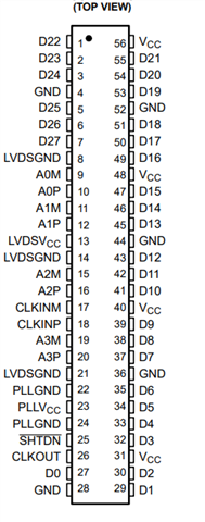
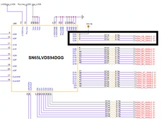
We would like to export the LVDS Signal to RGB output through your SN65LVDS94DGG

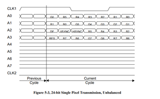
And, please let me know that which pin Hsync, Vsync, and DE Signal should be connected among the output signals of SN65LVDS94DGG.

( P.S. >>  I don't find those description of this pins in datasheet )

best regards,

hosung shin.

  • Hi Hosung,

    The output of the SN65LVDS94 is a 28-bit wide LVTTL bus. The output pins are D0-D27. Some of those pins are visible on the upper left of the diagram below.

    For mapping Hsync, Vsync, and DE, it will depend on which input it enters the SNLVDS94. Please refer to the diagram below for how the serialized data is split to the parallel output bus. 

    Regards,

    Jack Scherlag

  • Hi Jack,

    thanks you.

    Then, please let me know which pin RGB888 (24bits) maps to among D0 - D27.

    best regards,

    hosung shin.

  • Hi Hosung,

    Hsync maps to pin 24, Vsync maps to pin 25, and DE maps to pin 26.

    R0 -> D0

    R1 -> D1

    R2 -> D2

    R3 -> D3

    R4 -> D4

    R5 -> D6

    R6 -> D27

    R7 -> D5

    G0 -> D7

    G1 -> D8

    G2 -> D9

    G3 -> D12

    G4 -> D13

    G5 -> D14

    G6 -> D10

    G7 -> D11

    B0 -> D15

    B1 -> D18

    B2 -> D19

    B3 -> D20

    B4 -> D21

    B5 -> D22

    B6 -> D16

    B7 -> D17

    Regards,

    Jack