We have a query regarding the layout (signal routing) for this IC . I have attached two images below for reference.
The first image is from the datasheet of the part and as shown in the image, the DSI signal (ChA signals) enter from right and the LVDS signals for the same (ChA) exit from the left.
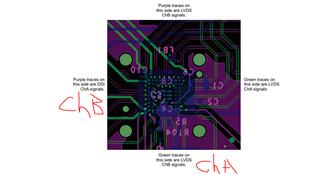
In our layout as shown in the second image, the DSI signals (ChA signals) enter from right side of the IC and the LVDS signals (ChA signals) exit from the top side of the IC.
The difference is that in the datasheet example the signals have adjacent entry and exit points while in our layout its not the same. Could you please provide a clarification regarding the same ? Are we missing any points related to routing for this IC ?