This thread has been locked.

If you have a related question, please click the "Ask a related question" button in the top right corner. The newly created question will be automatically linked to this question.

SN65DPHY440SS: DPHY440SS No Output from the MIPI retimer

Part Number: SN65DPHY440SS

Hi,

I'm working on a project that needs to send MIPI data over 22inches shielded twisted pair cable.  

I'm using a MIPI repeater board that uses DPHY440SS chip. I'm using a Omni sensor (1-lane MIPI). I connected the 1-Lane MIPI to the DA0P/0N and MIPI clock on the clock pins. 

I have no luck getting it to work. I see that the MIPI data pins are held at 1.2V and MIPI clock is 0V. I'm new to this chip. Please help me get this resolved.


Am i missing something? 

Thank you 

  • Hi,

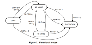
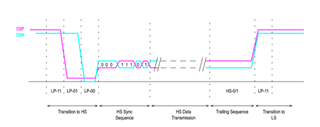
    1. The block diagram below shows the DPHY440 functional mode. To transition from LP to HS mode, you need to have the sequence LP-11, LP-01, LP-00. Are you seeing this sequence on the scope?

    2. Are you doing MIPI DSI or CSI? DPHY440’s LP TX is expecting to connect to an unterminated LP RX.  With Lane 0 path (DA0P/N and DB0P/N) supporting bi-directional LP signaling, it is very important that DB0P/N LP TX is connected to an unterminated LP RX.  If DB0P/N LP TX is connected to a HS RX, then LP signaling will not be able to reach the LP11 levels and which will cause the DPHY440 to not enable HS data path on Lane0.

    You can write the following registers bits to enable lane0 HS path. With this workaround, the Omni sensor needs to send HS data only. 

    Enable HS path for Lane 0 only:

    Write Register 0x50 with 8’h01 //Override enable for HS TX path

    Write Register 0x51 with 8’h01 //HS TX path enabled.

    Write Register 0x61 with 8’h00  // Disable LP path.

    Write Register 0x70 with 8’h01  //Override enable for HS RX path

    Write Register 0x71 with 8’h01  // HS RX path enabled.

    Bit 0 is lane 0

    3. You can also switch from lane 0 to lane 1, 2, or 3, which do not have the requirement of DB0P/N LP TX needs to be connected to an unterminated LP RX. In this case, you need to make sure the correct LP sequence is followed at the input as pointed out in the 1st bullet.

    Thanks

    David

  • Thank you. 

    How critical is setting up the EQ and ERC registers? I have EQ at 1.8V and ERC pulled to GND. 

  • Hi,

    EQ and ERC affect the signal conditioning only in HS mode. The fact that we are not even in HS mode would indicate to me a general setup issue.

    Thanks

    David

  • Hi David, 

    I ended up changing the lane from 0 to 1 for the data lane. now the MIPI data and clock lane on input and output are sitting at 1.2V

    Any thoughts?

  • Hi,

    This goes back to my first bullet. 

    1. The block diagram below shows the DPHY440 functional mode. To transition from LP to HS mode, you need to have the sequence LP-11, LP-01, LP-00. Are you seeing this sequence on the scope?

    The Omni sensor needs to drive the sequence LP-11, LP-01, LP-00 in order to go from LP to HS mode. Right now, it looks like it is just at LP-11 state (both P and N are 1.2V).

    Thanks

    David