This thread has been locked.

If you have a related question, please click the "Ask a related question" button in the top right corner. The newly created question will be automatically linked to this question.

DP83822I: 25MHz Clock Requirements

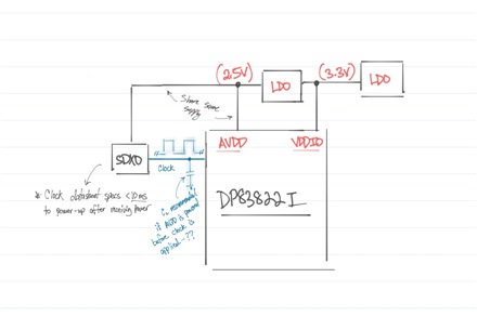
Part Number: DP83822I
Other Parts Discussed in Thread: CDCE6214, CDCE925,

The datasheet indicates when using XO/XI with a crystal, the crystal needs ~20pF load capacitance.
"Table 9-3. 25-MHz Crystal Specification" indicates 10~40pF for load capacitance. 

But when using an LVCMOS oscillator to supply the single-ended clock to XI (XO is left floating), 
"Table 9-1. 25-MHz Oscillator Specification" specifices a required load capacitance of 15pF~30pF.
Is this indicating you need to add an external capacitor between XI (pin23) and GND, between 15pF~30pF?

For reference, the DP83867 says XI/XO crystal needs an 18pF load capacitance;
But for XI (LVCMOS oscillator) input, if the voltage is 1.8V, a direct connection is all that is needed; no "load capacitance" is required.

Can you confirm the LVCMOS oscillator load capacitance requirements please?

Regards,
Darren

  • Hello,

    These specs look correct.

    Sincerely,

    Gerome

  • Hi Gerome,

    Please clarify for me...
    Does this mean when using a single-ended CMOS clock for DP83822 you need to add an external capacitor to the XI pin (pin23)??
    It appears to be a mistake in the datasheet?

    Recall:
    1) Input Capacitance listed in the DC CHARACTERISITCS section lists 5pF
    2) There is no load capacitance requirement for 25MHz reference inputs (single-ended) in GbE PHY (DP83867) or clock generators like CDCE6214.
    3)  This E2E post discusses a similar topic about another device - the "load capacitance" requirement seems to be a mistake.

    Could you double check with design if we need an external capacitor on XI pin, which severely affects Tr/Tf of the CMOS oscillator's output waveform and makes finding an appropriate 25MHz clock very difficult.

    Also, the EVM has capability to support CDCE925 to test a CMOS clock on-board.
    There are no external capacitors between CDCE925 and the XIN pin of the DP83822.

    CDCE925 also has Tr/Tf rated with CL = 10pF (Figure 4 in CDCE925 datasheet); which is outside the DP83822I spec of >15pF.
  • Hi Darren,

    The capacitor is advised for specific use case where, PHY is powered up but clock is not available. To avoid noise getting picked-up, the capacitor was advised. If the clock is available ahead of Power supply ramp on your design, you can remove it.

    Sincerely,

    Gerome

  • Hi Gerome,

    I attatched the use-case below. Specifically...
    1) 3.3V is generated and provided to VDDIO
    2) After the 3.3V rail is up it powers an LDO to generate 2.5V
    3) This 2.5V goes to both AVDD and the clock; so they receive power at the same time
    4) The clock datasheet guarantees it will power-up within 10[ms] of 2.5V rail ramping.

    In this use-case, are the timings described in Table 7-7 and Figure 7-2 for an "unstable" XI clock required?

    Basically, if the clock is starting after AVDD then RESET needs to be toggled according to desribed timings, yes?
    If so, then because the device is held in RESET during all the power-ups / clock starting, the recomendation for the extra 15~30pF of load capacitance on XI goes away?

    LVCMOS clocks are spec'd for Tr/Tf at certain load capacitances. CL = 5pF is typical.
    What would need to be the Tr/Tf requirements and the CL measurement capabilities of the clock to support this DP83822 requirement?

  • Hi Darren,

    In this situation, the capacitors are not a must have, but the reset will be needed.

    Sincerely,

    Gerome

  • Hi Gerome,

    Understood.

    Just for clarity:
    The DP83822 gives a TYP input capacitance of 0.8pF for the XI/XO pins.
    Can you confirm the MAX value?
    (This "load capacitance" is the main design point to ensure the selected clock meets the Tr/Tf requirements)

  • Hi Darren,

    The max value is 1pF.

    Sincerely,

    Gerome

  • Hi Gerome,

    Quick follow-up. The COUT value (5pF typ) referes to what exactly?
    Is it the output capacitance of pins like TX_CLK and GPIO1, etc?

    Or is it how much loading capacitance these pins can experience and still output voltages within datasheet spec?

    Regards,
    Darren

  • Darren,

    This is output capacitance of our output pins.

    Sincerely,

    Gerome