


Hello TI Forum,
I've made a LGA to USB adapter for IoT modules.
For some reason the TUSB4020BI-Q1 draws alot of current from the 1.1 V LDO and it gets very hot. (And eventually breaks if supplied long enough).
I've so far only noticed one design miss that I've made:
I noticed this in the datasheet for TUSB4020BI-Q1: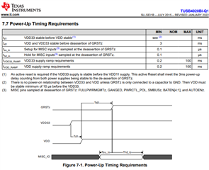
The way I read it is that LDO 1.1 V must be stable before LDO 3.3 V if GRSTz is tied to GND (which it is in my design).
Looking at the data sheet for my LDO 1.1 I see that it takes about 800 µs to start up:
While my LDO 3.3 V only takes 120 µs :
The proper way to solve this would then be to send the output of LDO 1.1 to the EN pin on the LDO 3.3 right?
But I'm unsure if this is the big error I've made here, I fear there is more.
I can't share the schematic openly due to company policy, but can I send it to a TI Guru for a review?
Any help would be greatly appreciated.
Best Regards,
Oscar
