Because of the Thanksgiving holiday in the U.S., TI E2E™ design support forum responses may be delayed from November 25 through December 2. Thank you for your patience.

This thread has been locked.

If you have a related question, please click the "Ask a related question" button in the top right corner. The newly created question will be automatically linked to this question.

TIOL111: 230.4kBaud Data Integrity Issue

Part Number: TIOL111
Other Parts Discussed in Thread: , , TIOL112, LM5160

We are having issues where the transceiver is behaving strangely over time. Below is the relevant schematic.
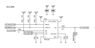


Our device is not responding to the IOLink master wake-up request - we should be using the 230.3kBaud COM3, but we are trying to determine why our device is not responding. Because we never respond the master repeatedly polls at each of the three baud rate options. Probing the data line into the transceiver compared to the data pushed out the RX pin of the transceiver, shows the expected output at slower two speeds:

COM1, input (IOL CQ data line) to TIOL111:
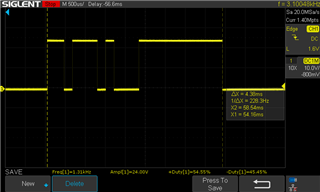
COM1, output (RX line from transceiver to microcontroller):
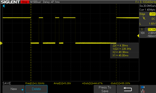

COM2, input to TIO111:
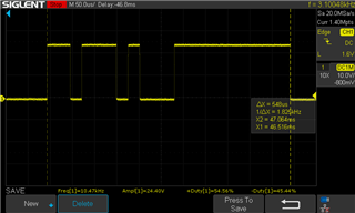
COM2, output from TIOL111:


However, at COM3, the transceiver RX output does not match the input that it is receiving:
COM3, input to TIOL111:
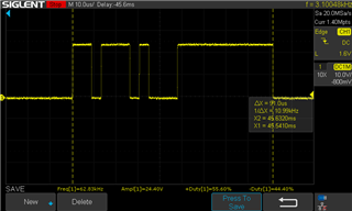
COM3, output from TIOL111:
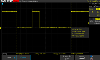

Are there any known issues with the device at COM3, or issues to be aware of, or any similar problems that have been experienced? This has developed recently and we have a very short deadline to resolve the issues for our customer.

Thank you.

  • Hello Matthew,

    I'm sorry to hear you are having difficulties.  No, there are no known issues with running the TIOL111 at COM3.  However I do have some questions and some thoughts on what may be the source of your issue.

    Can you confirm which version of the TIOL111 you are using?  Is it the TIOL111 (non-LDO version), TIOL1113 (3.3V LDO version, or TIOL1115 (5V LDO version)?  I see in the schematic that you have 3.3V connected to the VCCIN/OUT pin, but I don't know if this 3.3V is coming from an external supply, or being sourced by the TIOL1113 LDO.

    What confuses me is that your scope plots show the RX amplitude being roughly 5.28V, but this should match the VCCIN/OUT voltage which is shown to be 3.3V in the schematic.  So please confirm what version of the device you are using, and whether the 3.3V on the VCCIN/OUT is from an external supply.

    Can you tell me the value or scope plots of the TX, EN, nFAULT, and WAKE pins before and during this time when the Master sends the wake-up pulse and then follows up with a data packet?

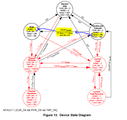
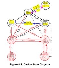
    It sounds like the EN pin may be low (Driver = off) when the Master sends the wake-up pulse.  If this is the case, then the device is already in the "Receive Only" State and the WAKE pin remains Hi-Z.  If the EN pin is High (Driver = on) when the Master sends the wake-up pulse, the device will transition to the "Wake" State and the WAKE pin will pull Low as a signal to the MCU to disable the driver (pull EN pin Low) to place the transceiver into the "Receive Only" State for the incoming data.

    There is some ambiguity in the IO-Link Standard documents about what is required of the WAKE pin when the driver is already disabled.  I know that many other IO-Link transceivers monitor for a wake up pulse even when the driver is already disabled and use it as a form of interrupt to the MCU as a signal data is about to come.  However, the standard doesn't define any specific behavior for this pin in this situation and it only defines the behavior for when the driver is on and would otherwise block data transmitted from the Master.

    If this is the situation you face and your device is expecting a WAKE pulse prior to receiving data from the Master in order to respond, then you may try to keep the EN = High during the idle time so that the Driver is enabled and ready for the Master to send the next wake-up pulse.

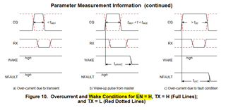
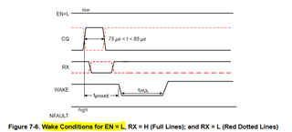
    We also have a newly released IO-Link transceiver (TIOL112) that changes this behavior to allow the wake-up pulse to be reflected on the WAKE pin even when the EN pin is low, the device is off, and the device is in a Receive Only state.  Instead of latching the WAKE pin low after receiving a wake-up pulse, the WAKE pin is pulsed Low for a short period of time which is compatible with most MCU interrupts that are edge triggered.  The TIOL112 was designed as an enhanced version of the TIOL111 and is footprint compatible with the TIOL111 and should be drop in replacement for most applications.  You may want to consider this device as well.

    Here are the plots for the WAKE behavior in the TIOL112 datasheet:

    Regards,

    Jonathan

  • Hi Matthew,

    Sorry for the second post, I realized I didn't comment on the RX waveform in COM3.  Understanding why the device is not recognizing the wake-up pulse is probably the key to get the system working and why I was focused on that in my first response.

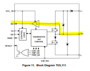
    The RX signal always reflects the CQ pin, and is just a level shifted version of the CQ voltage.  If the driver was enabled while the Master was communicating, this could impact and corrupt the waveform.

    We also need to verify the wake-up pulse in the COM3 mode is valid and of the correct duration (not too long or too short).

    Regards,

    Jonathan

  • Hi Jonathon,

    I appreciate your quick and detailed response.

    We are using the TIOL111, non-LDO version. The "3.3V" that is present on the VCCIN/OUT pin is a supply rail from elsewhere on the board.

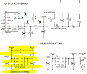
    The RX amplitude is misleading , it is a result of prototyping different configurations on this board. The main power source comes into the board from a 24V supply, and is stepped down using the LM5160 and a coupled inductor to form an isolation barrier. The LM5160 produces ~5V (amplitude you are seeing on RX pin). Across the isolation barrier, this is dropped down to 3.3V by the combination of the rectifier and LDO U4. On the primary side, the same LDO was populated on the board for testing, but is currently being bypassed because everything on the primary side of the barrier is tolerant of the ~5V output so the additional regulation to 3.3V is unnecessary. The data lines pass through a capacitive isolator, so the difference in the "3.3V" rails from one side of the barrier to the other doesn't cause an issue (the same signals are measured on the other side of the barrier with 3.3V amplitude without issue).  It isn't clear (I apologize for that) but the amplitude is expected. See schematic snip below:

    I don't have scope captures on hand of all, but I have investigated the other signals:

    -EN: Enable remains low at all times - your comment about the enable being low during the WAKE pulse is correct for our device.

    -nFAULT: Remains high at all times - no faults are detected.

    -TX: Remains high at all times - our device is not trying to respond, the received message does not prompt a response.

    -WAKE: When we started experiencing issues this was my first suspicion, but upon investigation the WAKE pin is not changing because the device is in its receiving state to begin with when it receives the wake-up pulse from the master. Additionally, the pulse measures between 75-81us (squarely within the specification), and the master waits for 510-530us after the wake pulse ends to start sending messages (also within the specification as I interpret it, in that devices are required to be ready to respond no later than 500us after receiving a wake pulse).

    The message from the master appears to be correct at all three COM speeds, we decode 0xA2, which is expected:

  • Would the transceiver be damaged if the driver is mistakenly enabled (EN=high) while the master is transmitting data?

  • Hi Matthew,

    Thank you for the clarification on the voltage levels.  I didn't think this was an issue, but while debugging I look for anything that doesn't look correct and assume it may be a clue. I understand what you are doing.

    Yes, the device board is expected to transition itself in to Receive Only mode within 500us of receiving the wake-up pulse.  The master will send the pulse and wait at least 500us before it sends the first test message at the COM3 rate and then it wait for a response from the device board within 27-33 Tbits (bit times at the COM rate).  If the device board has not responded, the master will send the next test message at the COM2 rate, and then again at the COM1 until it gets a response, or it times out and repeats the entire wake up sequence.

    The device board shall only support one of the COM rates. So if  you are trying to communicate at COM3, your MCU UART should be configured to support 230.4kbps and the MCU needs to respond to the master within 117.18us (min) to 143.22us (max) based on the 27-33 Tbits for COM3.

    Since the TIOL111 is a simple device, it will not respond to the master by itself, and the UART frame from the master will need to be detected by the MCU and then an appropriate response UART frame sent back to the master.  With the EN pin low, the TIOL111 will keep the WAKE pin Hi-Z but it will still pass the data to the RX pin.  Is your MCU constantly monitoring the UART port for a message from the master, or does it require some activity on the WAKE pin to prepare itself to receive a message from the master so that it can respond within the 27-33 Tbit response time?  Typically when I get wake up related questions, it is because the MCU requires a transition on the WAKE pin to be used as an interrupt and prepare itself for the incoming message, and without this WAKE pin transition, the MCU misses the message and doesn't respond in the required time. So I'm curious how your MCU is configured and if this is somehow responsible for your board not responding to the wake-up request.

    To your other question, the device will not be damaged if the driver is enabled (EN=High) while the master is transmitting.  From a physical layer perspective this is the same as how the master transmits a wake up pulse while the device is transmitting. 

    I'm still a bit confused about your original scope plots for the COM3 waveforms.  RX should always follow the CQ pin and therefore these waveforms should be the same.  Because the driver is disabled (EN=Low) this should not interfere with the waveform on the CQ pin coming from the master.  Can you probe both the CQ and RX signals at the same time?

    Regards,

    Jonathan

  • John -

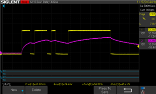
    We found something interesting probing this device. We probed on either side of R58 in the schematic I originally posted - it is a series 10ohm resistor in series with the CQ line. This was originally added for testing as a general current limiting measure, it is a standard element that we add to Modbus and Canbus lines in the same fashion.

    Channel 1 (yellow) is on the incoming side of R58 (the right side in the schematic capture posted, which is directly from the master). Channel 2 (purple) is on the left side of R58 (between the series resistor and the transceiver):

    Removing and shorting R58 corrects the issue - is there a reason that this resistance causes such a dramatic issue?

  • Hi Matthew,

    Well, without knowing some of the specifics, or doing any type of tests of my own, this looks kind of like a standard RC time constant type of situation where the resistance and capacitance of the cable and board traces is adding to the 10 ohm resistor.  I would think that the master's transceiver would have a decent current drive capability, but series resistors are not typically found in on the CQ line between the master and Device.

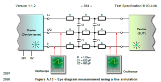
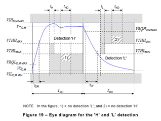
    Here is the test circuit from the IO-Link Test spec used to certify the physical layer voltage and waveform parameters or "eye diagram".  This network configuration is used to simulate a 20 meter cable connected between the maser and device.  the resistors are 1 ohms each to represent the parasitic resistance along the PCB trace, connectors, and cable in a real system.  But that is only 3 ohms total, compared to the 10 ohm resistor on your board.

    I'm glad you have it working now.  Thanks for letting me know.

    Regards,

    Jonathan