This thread has been locked.

If you have a related question, please click the "Ask a related question" button in the top right corner. The newly created question will be automatically linked to this question.

SN65MLVD203B: D line pulls down logical signal

Part Number: SN65MLVD203B

Hello,

I had some questions a few weeks ago in this forum theme:

https://e2e.ti.com/support/interface-group/interface/f/interface-forum/1089599/sn65mlvd207-bidirected-signal-with-one-wire/

I did some changes in my schematic and now I have a new issue.

I want to give a short introduction to my schematic:
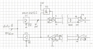
A logical signal will be sent from “data A2 via the bus driver “74LVC2G125” (U3). Then the signal should go into the D input from a SN65MLVD203B (U1.1). The chip U1 is connected to a corresponding device U5 with the same logic constellation as U1. (that’s why I did not draw the logical side from U5). U2 is therefore to allow only transmitting signals via the D input from U1.1 when nothing will be received via the R line from U1.2. The bus drive U4 serves as a diode so that the signal can only be transmitted in one direction.

My problem is the R line input from U1. First, I had the schematic without U3, but it looks for me that the D line pulls down any kind of logical signals. To be sure I added the U3 chip.

I made a screenshot from my oscilloscope:

On the blue channel a logical signal from a microcontroller can see (3.3V). The red signal is the output from U3 and so also the input level from the D line. For me it is not clear why the logical signal is so much lower than the data A signal. Before I add the bus driver U3 I used a frequency generator and I have to increase the frequency output voltage up to 4.5 volts to get a 3.3V input signal on the D line.

So, my thought is that the D line from U1 pulls the signal down to 0V.

Does someone have an idea why this could be? Is my SN65MLVD203B maybe damaged? But therefore, I changed the chip with a bread new device and then I get the same result.

Best regards,

Marcel

  • Hi Marcel,

    When you changed the chip, did you also supply 4.5V? If so, note that this is above the recommended operating condition as well as the abs max rating per the datasheet.

    Also double confirm the LVC device is configured per the OE, as an output for U3 and as an input for U4. However, do you have the Receiver and Driver in the opposite direction for bus contention by any chance? If so please see, How to Support 1.8-V Signals Using a 3.3-V LVDS Driver/Receiver + Level-Shifter to further help with the implementation, thanks.

    Best Regards,

    Michael.

  • Hello Michael,

    I have never connected 4.5 volts to the SN65MLVD203B. I have to increase the internal frequency generator up to 4.5 volts so that I have 3.3volts on the D pin. I placed a measurement line on the oscilloscope. So I can never set a voltage higher than 3.3 volts. (Those are the two dashed lines on the blue signal) It looks like as if a low-impedance connection exist on the D pin to GND.

    The OE pins from U3 and U4 are connected to GND and so they are always active.

    As I wrote once a microcontroller signal was connected directly to pin D (5). As soon as I connected this signal to pin 5, the 3.3V voltage dropped below 2V. That is why I add the U3 chip so that the microcontroller signal is stable to 3.3V. But then the output voltage from U3 drops below 2volts. The chips U1 and U5 have exactly the same wiring. I have created two tests boards:

    Complete environment with microcontroller board:

    The source voltage for all three boards are 3.3V from an power supply.

    I can not explain why the voltage collapses below 2 volts.

  • Hi Marcel,

    Could you help share the full schematic?

    However, please also help compare your termination to the recommended 50-Ohms for MLVDS devices as well, thanks.

    Best Regards,

    Michael.

  • Hi Marcel,

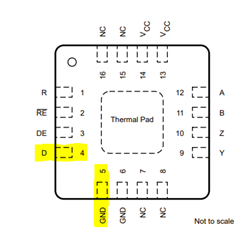
    In addition, could you help double conform if you are using 203 or 203B? If 203B, please note the below pinout, thanks.

    Best Regards,

    Michael.