This thread has been locked.

If you have a related question, please click the "Ask a related question" button in the top right corner. The newly created question will be automatically linked to this question.

DS90UB964-Q1: Application problems of chips

Part Number: DS90UB964-Q1

Regarding ti's 960 and 964, I would like to ask the spec that the minimum rising edge time of Vdd and VDDIO should be 200ns. If this index is not met, what will be the negative impact?

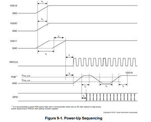
There is another problem, that is, regarding the power on timing of 960 and 964, I don't know if there is a clear sequence requirement. Look at the spec, 964 says that the minimum time of power on t0, T2 and T4 from vdd11 to VDD / VDDIO is 0ms, and the legend indicates the time from the power supply stabilization; However, it is written in 960 that the minimum time from VDD / VDDIO to vdd11 is 0ms, but the legend indicates the time from 10% of the power supply

  • Hi Tony,

    Thanks for your inquiry. With regards to the minimum rise time of VDD18, VDDIO, these timings should be strictly followed to allow the deserializer to be initialized in a deterministic state.

    In this case, it appears that the power-up sequence for the DS90UB960 is more clear than the DS90UB964. For your application, we would recommend that the DS90UB960 power up sequence be followed also for the DS90UB964. For the figure 9-1 below in the DS90UB960 datasheet, the t0 timing should be from 90% VDDIO/VDD18 to 10% VDD11. This will ensure that VDD11 comes up after VDD18/VDDIO as intended.

    Best,

    Thomas