A related question is a question created from another question. When the related question is created, it will be automatically linked to the original question.
If you have a related question, please click the "Ask a related question" button in the top right corner. The newly created question will be automatically linked to this question.
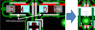
It's hard to tell if this is optimal placement since this image is very zoomed, if you can provide a more zoomed out image I can provide better feedback.
The best placement is as close to the ESD source or connector as possible.
Make sure unprotected circuits aren't close to the trace between the ESD source and ESD diodes to minimize EMI.
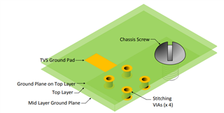
The TVS ground pin should connect to a same layer ground plane that is coupled with another ground plane on an immediately adjacent layer. These ground planes should be stitched together with VIAs, with one VIA immediately adjacent to the ground pin of the TVS. Below is an example:
Is it best to connect the GND by inserting one GND VIA between the signal lines (Ex. USB SS)?
You want to avoid VIAs between the ESD source and the TVS IO pins.
The best way to connect the TVS GND is depicted in the image from my first reply. You want to connect the TVS GND pin to a same layer GND plane, then use VIAs to connect to an adjacent internal GND plane.
Use a grounded chassis screw to connect the PCB ground and position it near the TVS and ESD source as the connector ground shield.
Also, use VIAs witha large diameter and large drill to lower impedance.
I understand the document you sent. However, in the case of ESD122, I think that it is impossible to connect to GND on the same plane due to the data lines passing left and right.
Q)
1. Is there any other way other than putting the GND Via between the data lines?
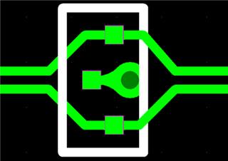
2. Is it ok to place the GND VIA under ESD122 as shown in the picture below?
2. Is it ok to place the GND VIA under ESD122 as shown in the picture below?
I would place the via on the GND pin or to the left of the GND pin where the traces are connected to the rest of your system, not on the side between the ESD source/connector. (I'm assuming the traces to the right connect to the ESD source).
I would also recommend to run a thicker trace from the GND pin to the VIA or just placing the VIA on the GND pad.
You should then connect this via to an internal adjacent ground layer to keep ground shifts at a minimum.