This thread has been locked.

If you have a related question, please click the "Ask a related question" button in the top right corner. The newly created question will be automatically linked to this question.

DP83826E: The control MCU cannot read DP83826's register

Part Number: DP83826E

Hi team

I’m Joe form GZ office, my account is SAJ. When my customer use DP83826 to replace DP83822 there is a very confused problem.

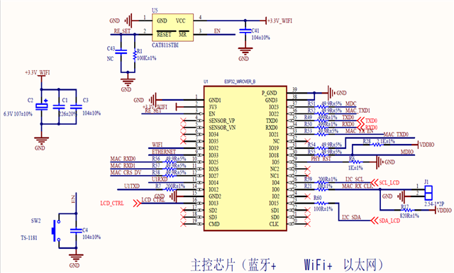
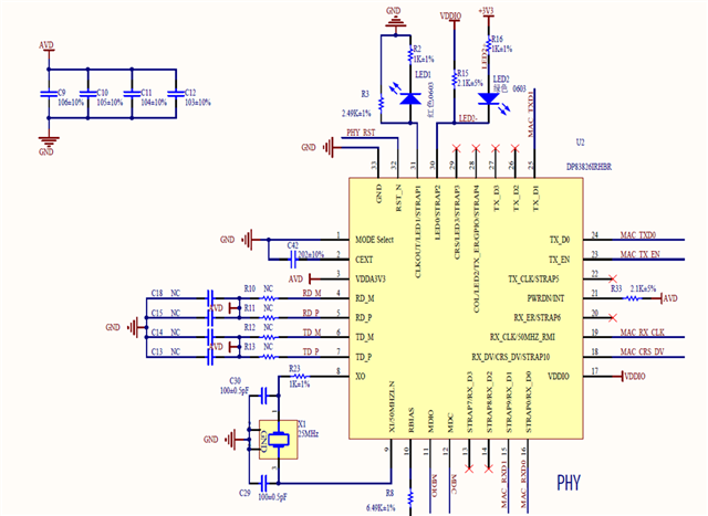
In this application DP83826 works on RMII Master Basic mode, the PHY address remains default.

The following pictures are the application circuit of DP83826. I have checked with customers many time, there is no problem on the connection. The voltage of each Pin is normal.

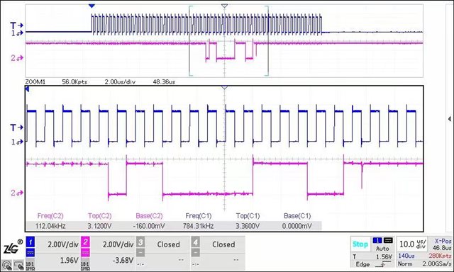
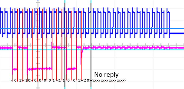
But after the MCU sends the massage and try to communicate with DP83826 through MDIO and MDC to read the register of it, there is no reply by DP83826, the following is the waveform of MDIO and MDC.

Could you please help me check this problem ASAP, the deadline of this project is closing. I and my customer have already checked for one week, thank you!

Thank you 

BR

Joe

  • Hi Joe,

    Is there any issues with link or data transfer? Or is it only Register access? Can you confirm the desired PHY address and check if the straps are reflecting that desired configuration.

    Please check the constrain mentioned in Figure 8-1 of Datasheet (T1-T4) are met.

    Regards,

    -Alvaro

  • Hi Alvaro

    I'm not sure if there is any link or data issue, because after the PCB is done, customer want to change some setting in registers before using, but we failed on the first step.

    The PHY address setting remains default, in basic mode, the address is configured by strap7(1) strap8(0) strap9(0), I have check the corresponding pin, the voltage Is correct.

    To fulfill the time limitation in figure 8-1, we not only sends the read request once, but periodically, there is always no reply form PHY. I have check that the clock of Pin8 and Pin9 is stable, and the output clock of Pin19 is also stable, they equal to 25MHz.

    A question: DP83826's PHY address has three bit binary, but the protocol format of table 9-3 has five bit binary in address, so what and where should I write in the rest of two bits ? Is the format <xx001> or <001xx> and x=1 or 0?

    Thank you and have a nice weekend!

    Joe

  • Hi Joe,

    Good catch, I understand how that can be confusing.

    The 826 can support 8 PHY addresses. So it is only 3 bits, 0-7.

    As for the rest of the issues, 

    Check if PHY is coming out of RESET

    • You can check this by pulling the  Signals from TX/RX CLK 

    Regards,

    Alvaro

  • Hi Alvaro

    PHY is not in reset mode, the output clock frequency of pin19 is 50MHz.

    I notice that in 826 Pin21 PWRDN/INT is different from 822's Pin8. Does that mean when I want to read the registers, Pin21 must be pulled down, otherwise I cannot read any data from register?

    But after I pulled down this register, the waveform from MDIO is the same as before.

  • Hi Joe,

    If RX_CLK is showing 50 mHz, that means the device is active. Which is good news.

    You mentioned the device is in RMII Basic Mode, the PHY Address pins are RX_D1, RX_D2, RX_D3; in that order, with RX_D3 as the LSB

    RX_D3 & RX_D2 are NC, so they retain their default values.

    Are we sure RX_D1 is not being driven high? Is the PHY ADD 0b001 confirmed?

    Is this the same ADD used for MDI Reg commands?

    Also, 

    Try probing PHY side of the MDI lines. 

    Regards,

    Alvaro

  • Hi Alvaro

    Thank you for help! Is there some software demo for customer to accelerate their development?

    Thank you

    Joe

  • Hi Joe,

    Unfortunately we do not.