This thread has been locked.

If you have a related question, please click the "Ask a related question" button in the top right corner. The newly created question will be automatically linked to this question.

SN65DSI84: Schematic review and some questions of REFCLK pin

Part Number: SN65DSI84

The LVDS clock can be derived from the DSI channel A clock, or from an external reference clock source.

The frequency of LVDS of our selected panel is as follows,

We use I2C interface select reference clock source and terminate to GND with a 4.7kohm pull-down resistor. Will REFCLK pin reference our panel LVDS clock 71.2MHz?

Also, if we use an external OSC 38.4 MHz, is there anything we should be careful about?

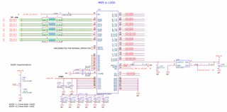
Schematic is as below, please help to check.

Thanks a lot.

  • Hi Jod,

    You can use either the internal DSI clock or an external reference clock as you pointed out to generate your LVDS clock.

    For the case where you use the 4.7kohm pull-down resistor on REFCLK pin, the internal DSI clock should be used. You can calculate what the suggested DSI clock frequency is with the DSI tuner tool and this video https://training.ti.com/configuring-sn65dsi8x-single-channel-dsi-dual-link-lvds-operation.

    If you use an external OSC 38.4 MHz, the source of the reference clock should be placed as close as possible with a series resistor near the source to reduce EMI and use the DSI tuner tool to select the correct configuration with your selected OSC frequency.

    Thanks,

    Zach