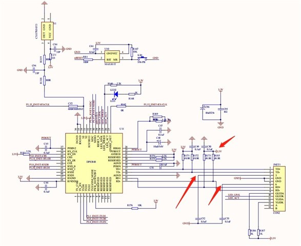
Part Number: DP83848I
Hi,
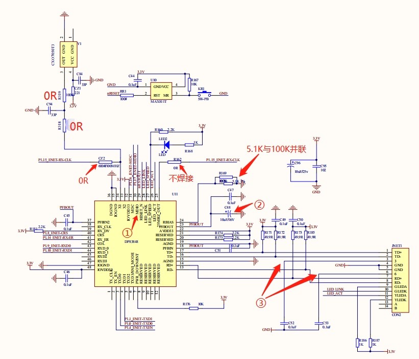
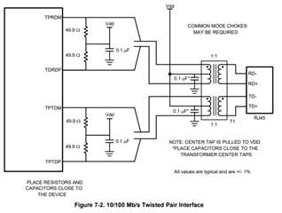
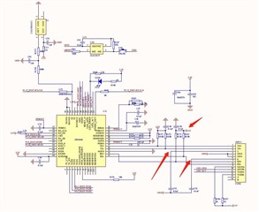
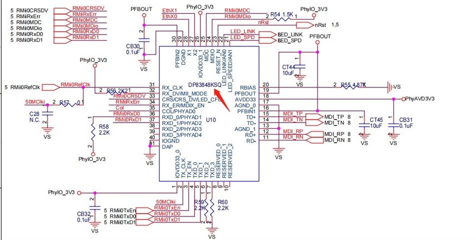
1. The above picture is about the principle design of this PHY chip. The Chinese characters and parameters are the actual welding values of the PCB board.
Label ①MDIO pin is not connected with 1.5K pull-up resistor
Label ② The 10UF with polar capacitor here is the actual welded 10UF/25V in-line electrolytic capacitor
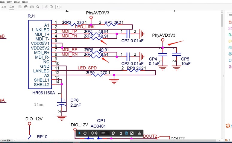
Does the center tap of the transformer need to connect to 3.3V power supply here?
Then, packet loss and sending delay are found on the IP address of the ping network port. Will the above comprehensive schematic design (①, ②, ③) affect packet loss and delay? In the schematic diagram, C94 is not welded on the PCB board.
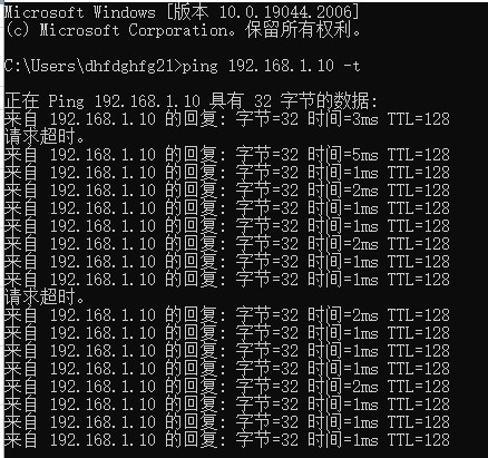
2.
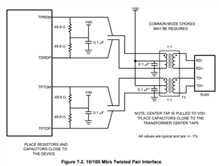
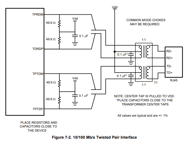
This PHY83848KSQ network transformer ① differential wire is 49.9R and capacitive grounded; ② The center tap is connected to 3.3V

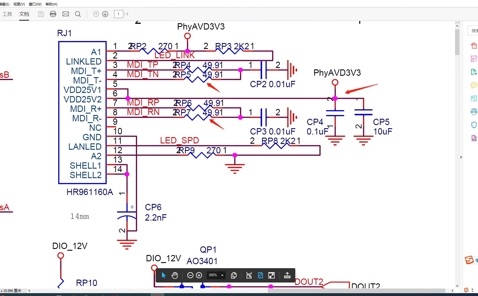
This PHY83848VVVBI network transformer is connected to differential wires through 51R to 3.3V. The center tap is grounded through a 0.1UF capacitor. Which of these two is correct for this type of PHY?
Thanks!


