Part Number: DP83825I
Hello,
My customer is designing the DP83825I.
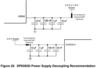
1. Please review the following schematic.
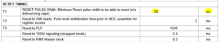
2. Below is the reset min timing in the DS. Is that time mandatory?
Thank you.
JH
Part Number: DP83825I
Hello,
My customer is designing the DP83825I.
1. Please review the following schematic.
2. Below is the reset min timing in the DS. Is that time mandatory?
Thank you.
JH