This thread has been locked.

If you have a related question, please click the "Ask a related question" button in the top right corner. The newly created question will be automatically linked to this question.

PCF8575: Use PCF8575 as input

Part Number: PCF8575

Dears,

Thanks for your support in advance.

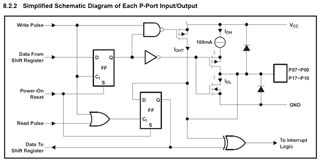
1. Below is the Block Diagram of PCF8575 from datasheet( I marked 1,2,3 three MOSFETS,), in my understanding this P-port is push-pull output (MOSFET2 and MOSFET3),

my question is: when configure PCF8575 as input port, how the MOSFET works?
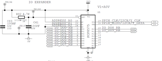
2. Below is the schematic of my application, PIN10-11,PIN1-8 were used, PIN12-PIN17 were not used

my question is: If all P-ports are used as input, whether PIN12-PIN17 can be left floating, or should be connected to GND(directly or by a resistor(what the value should be))?
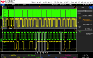
3. Below is the I2C waveform of my circuit, byte1 is:01000011,byte2 is:01111111, byte3 is11111111 (for byte1 is from Master, and every time master send 01000011, PCF8575 will send back PIN1-8,PIN10-17 condition, )

my question is: Whether byte1:01000011 can configure PCF8575 P-port as input port?
  • The PCF has quasi-bidirectional I/Os. This means that they can strongly drive low, but only weakly pull high. The direction cannot be configured directly; to use a pin as input, configure it to output high (which is the default).

    1. MOSFET 1 strongly drives high when the register is written. This happens only for a short time. MOSFET 2 weakly drives high (the current source actually is 100 µA). MOSFET 3 drives low.

    2. Unused pins can be left open; the internal pull-up prevents them from floating.

    3. The first byte contains the device address, and the R/W bit. When reading, the PCF always returns all 16 bits.

  • Hi Yixiang,

    1. Below is the Block Diagram of PCF8575 from datasheet( I marked 1,2,3 three MOSFETS,), in my understanding this P-port is push-pull output (MOSFET2 and MOSFET3),

    my question is: when configure PCF8575 as input port, how the MOSFET works?

    Your understanding is correct. P-port is push-pull configuration. Upon initial power up of the device, I/O's are defaulted HIGH by current source 100uA current source (says 100mA in datasheet, this is an error). 

    MOSFET 1: Used as a strong pull-up to VCC when an output is written HIGH and is switched off by the negative edge of SCL. 

    MOSFET 2: Weakly drives HIGH through 100uA current source to VCC. 

    MOSFET 3: strongly drives LOW

    2. Below is the schematic of my application, PIN10-11,PIN1-8 were used, PIN12-PIN17 were not used

    my question is: If all P-ports are used as input, whether PIN12-PIN17 can be left floating, or should be connected to GND(directly or by a resistor(what the value should be))?

    Unused pins can be left open since internal 100uA current source pulling up to VCC is present. 

    3. Below is the I2C waveform of my circuit, byte1 is:01000011,byte2 is:01111111, byte3 is11111111 (for byte1 is from Master, and every time master send 01000011, PCF8575 will send back PIN1-8,PIN10-17 condition, )
    my question is: Whether byte1:01000011 can configure PCF8575 P-port as input port?

    P-port are initially configured as input upon power up. Write to device register using 0x66 (01000010) to configure P-ports as input or output. 

    Regards,

    Tyler