Because of the holidays, TI E2E™ design support forum responses will be delayed from Dec. 25 through Jan. 2. Thank you for your patience.

This thread has been locked.

If you have a related question, please click the "Ask a related question" button in the top right corner. The newly created question will be automatically linked to this question.

SN65HVD52: [KORTEK]] Inquiries about abnormal operation of SN65HVD52DR

Part Number: SN65HVD52

Hi, TI support team

The following inquiries have been received from customers.

This is an inquiry about abnormal operation of SN65HVD52DR.

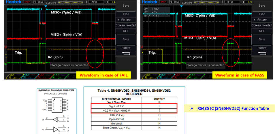
1. The signal of R output (2pin) is output differently according to the difference of 7,8 pin input signal of SN65HVD52DR (RS-485 IC). What is the cause?

2. In the function table of the data sheet, -0.2V<VID<-0.02V is marked as OUTPUT (R)->? What does "?" mean?

3. Does the differential input signal need to overlap for stable operation?

See picture below.
Thanks.

Regards,

MJ

  • Hi MJ,

    1. Can you possibly share a schematic so that I can check the design of the IC - I only really need to see the circuitry around the RS-485 device - if you can't I understand. Also can you confirm that the MISO+/MISO- voltage levels are the same in both pictures - or is there an offset? 

    2. The Question mark (?) means indeterminate state - which means it could be anything when the voltage is held in-between those bounds (usually manifests itself through glitching of the data if input differential voltage is within the stated range) 

    3. For valid voltages RS-485 devices require >= 200mV register as a high voltage and <= -200mV is a low voltage (from RS-485 standard) - from the scope shots it does look as if the differential voltage is > 1V at the very least - so I don't think the issue is necessarily due to the A and B signals not "overlapping".

    As of now I am not too sure what is the exact problem - if you could provide a schematic snippet it would be very helpful as its hard to diagnose the system without understanding how it is connected.

    Best,

    Parker Dodson

  • Hi, Parker

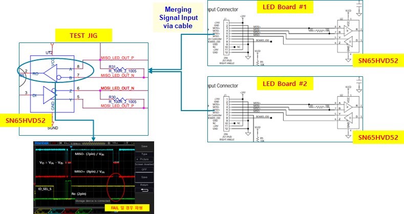
    I share the circuit diagram as below.

    Please confirm.

    Please let me know if you need anything more.

    Thanks.

    Regards,

    MJ

  • Hi MJ,

    Thanks for the additional information!

    So based on the schematic alone there are a few smaller issues - but I am not sure if they are actually causing the issue itself.

    Some potential issues or points of clarification:

    1. Configuration -does the differential bus split into two cables - or is there 1 cable between the two end nodes? This setup depending on implementation could result in some pretty major interference as if it is two cables (or one cable where the nodes deviation from the main electrical path is too long to be neglected based on the rise time of the signal) the system may  not be impedance matched and reflections are possible. This isn't as big of an issue if the electrical length of the circuit  is smaller than 1/10th of the signals wavelength. How long is the cable - and what data rate are you running at (max)? 

    In general the best approach is to daisy chain the devices. 

    2.  The termination resistor - 

    For RS-485 devices each differential bus should have two termination resistors, one at each end of the bus (for full duplex that would be 1 on the driver and 1 on the last receiver on the bus - if multiple transceivers exist on the same bus - only  two are terminated - but the unterminated nodes cannot deviate from the main transmission line  by more than L - where L = 1/tr * c * v - where tr(min) for this device is 120ns, c is the speed of light, and v is the propagation velocity of the medium (many cables are around 75%). The termination resistors should be 120 Ohms - as with both termination resistors that gives an effective impedance of 60 Ohms which gives a margin of 10% error (as RS-485 standard states a minimum of 54 Ohms of differential impedance). Using 100 Ohm resistors will violate the 54 Ohm specification and could cause the driver to become overstresed and have lower voltage outputs.

    3. Where does the wire go that is off page from Pin 8 (A) in the above diagram - any connections to this pin can impact the output voltage. 

    4. What is the trigger signal (yellow trace) used for/connected to? 

    Can you also let me know the part markings for a good part and a bad part? 

    So there are a few issues with the schematic - but I am not sure if they are critical - as a lot of the violations just add risk - not necessarily guarantee failure. I am a bit curious on the trigger signal as it seems to be slightly correlated to the output data - but it may just be a coincidence. If possible can you get a scope shot of Pin 8 - Pin 7 of the suspect device as well - I think it should fine but I want to double check. I am also going to check the part numbers and see if there could be a potential issue there. I am also concerned on what is connected to the A pin because that can directly impact the signal received.

    Please let me know!

    Best,

    Parker Dodson