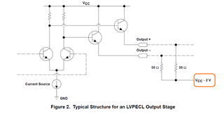

(1)Why can use (VCC-2V) to connect ?
(2)Why Output+ and Output- 's VCM=2V?
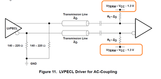
(3)Why AC-coupled VTERM=VCC-1.3V or not VCC-2V ?
This thread has been locked.
If you have a related question, please click the "Ask a related question" button in the top right corner. The newly created question will be automatically linked to this question.


(1)Why can use (VCC-2V) to connect ?
(2)Why Output+ and Output- 's VCM=2V?
(3)Why AC-coupled VTERM=VCC-1.3V or not VCC-2V ?
Hi,
(1)Why can use (VCC-2V) to connect ?
Driving a load that is referenced to a supply 2 V below the device supply assures that the final transistor stages in the output driver are always on. A Thevenin load is often used to create a 50-Ω effective termination, at a common-mode voltage 2 V below the local supply rail. Many other implementations have been used. The key to the specific load that is implemented lies in the understanding that the ECL driver output stage is a voltage driver, with the output voltage always referenced to the positive power rail for the device. The load that is driven must ensure that the final transistors on each output leg are in the active regions at all times.
(2)Why Output+ and Output- 's VCM=2V?
This is to meet the LVPECL receiver common mode voltage requirement of 2V.
(3)Why AC-coupled VTERM=VCC-1.3V or not VCC-2V ?
This is to establish the LVPECL common-mode voltage of 2 V at the receiver.
Thanks
David