This thread has been locked.

If you have a related question, please click the "Ask a related question" button in the top right corner. The newly created question will be automatically linked to this question.

SN65DP159: No response of SN65DP159 IIC interface (SCL/SDA_CTL)

Part Number: SN65DP159
Other Parts Discussed in Thread: SN75DP159

Hi,

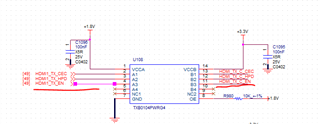
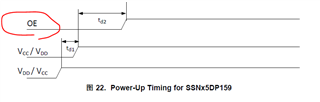
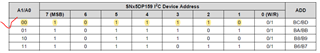
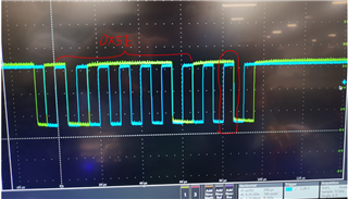
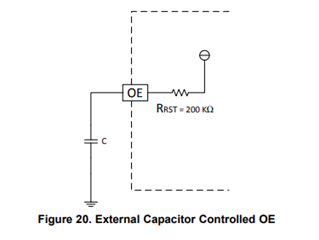
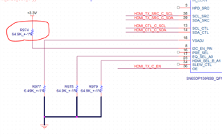
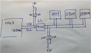
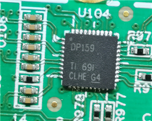
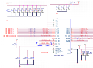
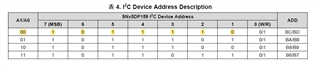
During accessing control IIC interface of SN65DP159, I found no any response from this IIC interface. So, I used oscilloscope to test SCL and SDA , and ninth data is not low that means I can't receive ACK signal from SN65DP159 . I interpret the IIC device address from the test curve on the oscilloscope, and it match first address in the address table. Then I test VDD and VCC, and they are all right.  The schematic is shown below, it almost copy the official design. 

Could you please help me check  this issue ? Any information will be appreciated.

Thanks in advance!!!

Best regards!!!

Jason

  • Jason

    How are you driving the OE pin? Do you make sure the power-up sequence is correct?

    Which I2C address are you using? Are you writing to DP159 with address of 0x5E?

    Do you have the pullup on SDA_CTL and SCL_CTL?

    Thanks

    David

  • Hi, David:

    Please see my response as below listed:

    1. How are you driving the OE pin?

    [Jason]: 1.8v bank of FPGA output OE -> 1.8V to 3.3V level shift ->  SN65DP159. The below figure show the level shift. And I test OE signal, it is high which means normal operation

    2. Do you make sure the power-up sequence is correct?

    [Jason]: Is this power-up sequence  very important for SN65DP159? Frankly I don't notice this requirement. This sequence will impact the IIC accessing?

    I will test this power-up sequence today.

    BTW,  there is sequence between VCC and VDD? As below figure shown, it seems that they have no sequence requirement

    3. Which I2C address are you using? Are you writing to DP159 with address of 0x5E?

    [Jason]: Yes, I use the address of 0x5E which is selected by EQ_SEL/A0 and HDMI_SEL/A1, and these two pin are pull down by 64.9K resistor

    4. Do you have the pullup on SDA_CTL and SCL_CTL?

    [Jason]: Yes, I do it. It is necessary!

    Best regard!

    Jason

  • Hi,David:

    After power on, we will give a reset to OE pin of DP159, and I think its effect is similar to the power-up sequence

    Also, no any feedback from IIC interface of DP159 as below figure shown.  You can see that the level is high at the ninth clock which mean DP159 don't give out any response. 

    Any information will be helpful. Thanks in advance!

    Best regards!

    Jason

  • Jason

    Can you change the reset so instead actively driving the OE pin, you will just have a 0.22uF pulldown capacitor on the OE pin as shown below?

    Can you also verify you have a 65k pullup on the I2C_EN?

    Do you have any other devices on the I2C besides the DP159?

    Thanks

    David

  • Hi,David:

    yes, there is a 65k pullup on the I2C_EN as below figure shown

    The topology is like below. There are three devices in the chain. Level shift is TCA9517ADGKR from TI too. Clock device(Si5324) on the chain could be configured  through IIC. But DP159 don't have any response as mentioned in the above post. I even remove the EEPROM to reduce load effect on the IIC, but the issue is still there.  3.3V and 1.13V are available for DP159 too. My board have two circuit like this, that means support 2 HDMI2.0 port. But two DP159 all have no response. I replace SN65DP159 with  SN75DP159, but issue is still. This problem is very strange. 

    I also check the other reference board which also connect the DP159 to FPGA directly without 0.22uF capacity in it. It can work good.

    Any information will be helpful. Thanks in advance!

    Best regards!

    Jason

  • Jason

    Can you remove both the Clock device(Si5324) and the EEPROM and see if DP159 will respond?

    From the schematic I do not see any issue that will cause DP159 not responding with ACK.

    Thanks

    David