This thread has been locked.

If you have a related question, please click the "Ask a related question" button in the top right corner. The newly created question will be automatically linked to this question.

TLK2711-SP: Regarding the integrated interfacing of multiple TLK2711 to use as serializer and deserializer

Part Number: TLK2711-SP

Hello support team,

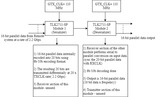
Please find attached reference block diagram for the TLK2711-SP. We are thinking to use 2 different TLK2711-SP out of one module will be used as a serializer and another module as a deserializer. Is the below block diagram is correct to receive accurate data at the output of module-2. What are the factors we need to take care so that we don't face any problem like bit misalignment, missing data? could you please provide some guidance. 

Also, do we need to synchronize the both GTX CLK for this kind of multiple module of TLK2711-SP? 

Awaited your feedback and response. 

  • Hi Maitry,

    Thanks for sharing your block diagram.  In general, this would be an appropriate application for this device.

    In terms of design considerations to watch out for, there are a few that come to mind.  In general, it is worth reading through the datasheet to ensure that nothing critical is overlooked.

    • You will need to meet TXCLK requirements (see below).
    • I would recommend reading through "8.3.12 Comma Detect and 8-Bit/10-Bit Decoding".  This will be important for bit aligment.
    • I would also recommend reading through "8.3.20 Power-On Reset".  Note that active transitions are required on the receiver to correctly reset the device and lock to incoming data.  This means that your transmit device will need to be transmitting data while resetting the receiving device.

    GTX clock does not need to be synchronized between the devices.  The receiver will generate a recovered clock from the serial data.  However, GTX_CLK does need to be synchronized to your parallel transmit data TXD[15:0].

    Thanks,
    Drew