This thread has been locked.

If you have a related question, please click the "Ask a related question" button in the top right corner. The newly created question will be automatically linked to this question.

DS90CP04: About serial interface design

Part Number: DS90CP04

Hello, I have some questions, please help 
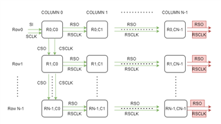
1.According to SPEC requirements, my understanding of the connection is shown in the figure. Please help to confirm whether RSO and CSO are connected correctly and appear in appropriate rows or columns.

2.If i want to read the config register value of the specified DS90CP04 device, shoule connect all the RSO and RSCLK of the last device in each row to the Host? and how about CSO and CSCLK of the last device in each row   (In red above)

3.According to your observation, is it necessary to draw out the serial interface for  read ,because we have so much rows. The host  pin  resource is  limited.

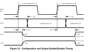
4.I don't quite understand the picture below, please help to explain:

4.1Are ConfigA and ConfigB two configurations in the same device? Doesn't a device theoretically have only one configuration  in Load register? My understanding is: for example, in the NxN matrix, all devices are successively written to the load register. So A and B are the same config, right? The second load rising edge is purely to open OUT, but the second  contents of the load register are the same, right?

4.2LOAD pin in L->H->L->H ,In the process of H state, except timing between OUT and  LOAD is considered(tsw,toff,ton),is there a requirement for the maximum duration of the LOAD signal's high level? And is there a maximum and minimum time requirement for a low level between two high levels? Because we want to use a low speed IO to control the signal, the LOAD frequency will not be too high.

4.3 After programming is completed, Can LOAD be pulled up at any time to transfer load register's content ?Any time?
5.In the crosspoint matrix, if the former stage DS90CP04 is connected to the next stage DS90CP04, is it necessary to add 100R end-resistor for LVDS at next stage DS90CP04?

  • Hi Chenglong,

    It is much easier to select different configuration through pins(MODE pin High)- versus serial connections. You can use GPIO to dynamically select different configurations. Given you are using serial configuration please note comments below:

    1). Yes your understanding is correct.

    2). You should connect the last RSO and RSCLK to the host. Then decode let host decode 30-bits frame or shift register.

    3). It is not necessary to draw out 30-bits configuration. Read operation is done just for checking the configuration.

    4). This timing diagram shows Tsw, Toff, and Ton parameters:

    Tsw is the delay before the new switch configuration goes into effect or before it becomes active.

    Toff is the active to tri-state delay

    Ton is the reverse of the Toff - time from in-active or tri-state to active delay.

    4.1). Configuration A and B are two different configurations for the same device.

    4.2).  Minimum LOAD width should be greater than max Ton(300ns).

    4.3). When LOAD is high, device uses its shift register content into its configuration register therefor switch configuration may change based on what was in the shift register. So after programming the device we should not assert LOAD since it could change the configuration.

    5). Yes we need to add 49.44 as shown in the test circuit(figure 4 of the data sheet).

    Regards,Nasser

  • Thank you for your reply

    Since we have 78 Crosspoint devices, we can't use GPIO to switch controls. I still have some questions in your reply, please help to answer them again.

    2. Should RSO and RSCLK of the last device in each row be routed(  (0,N-1);(1,N-1);.....;(N-1,N-1)  ) , or only the RSO and RSCLK of the last device in the whole matrix (N-1,N-1)?

    2.1 When reading registers, should CSO and CSCLK be routed on the same device as RSO and RSCLK

    4.2 Is there any requirement on the maximum duration of LOAD high level and low level? 

    4.3 Is there a maximum requirement for the time interval between the device programming and LOAD pull up?

  • Greetings,

    2). RSO and RSCLK of the last device in the matrix.

    2.1). When reading register, we should read the whole 30-bits from the last device in the chain as noted in #1 above.

    4.2). There is not a maximum duration of LOAD high. However, please note when LOAD is high and there are multiple SCLK transitions device will keep transferring its shift register into the configuration register. Also, there is not a limit on low level. When LOAD is low configuration register is not updated.

    4.3). When LOAD is high and after one SCLK configuration gets updated. Therefor we have to wait for one SCLK period before applying a new configuration to be loaded. 

    Regards,Nasser

  • 2&2.1

    I Read some description  in the "Read-back Switch Configuration" section:

    a. "Upon receipt of the special read start frame the configuration register information is transferred into the shift register and output at both RSO and CSO in the OUT1 to OUT4 bit segments of the read control word."

    b. The "relative" column address emerges at RSO of the last device in the row and is used to determine (11 1111' b-N) the column of the sending device. Similarly, the row address emerges at CSO of the sending device."


    It is mentioned that the CSO pin should be routed to host for completing  the read-back action. Are you sure do not need to route the CSO signal to host?

    and the RSO routed is only  the last device in the whole matrix ,not the last device in each row?

  • Hi Chenglong,

    You are correct we need both RSO and CSO.

    Also, as noted in page 14 table 4 of the data sheet with 4 devices cascaded the last device will shift out 148 bits - so this is from the last device. Given you have N-1 rows and N-1 columns, and these are cascaded by RSO and CSO, then the last device(row=N-1 and Column = N-1) will shift out all the columns and rows configurations.

    Regards,Nasser

  • Hi,Nasser,

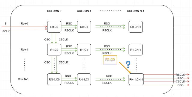
    1.  I have updated the block diagram according to the information we communicated, please Pay attention to that only the first column devices will be connected via CSO&CSLCK,all the other column devices 's CSO&CSLCK (except the last device of matrix) will not be used .And All devices will be  connected  throught  RSO&RSCLK.  Please  help to finally confirm whether it is correct? 

    2. According to your reply, I have another question. For example, in the figure (R1, C5) device, how is the read out data transmitted to the last device in the matrix and output ?   Since I understand that this device can only transmit data passes through its downstream device  in the row and not the column (if not connect the CSO&CSCLK is correct), I always thought that only devices (R1, CN-1) could read the information of all devices in this row 1.What did I do wrong?

  • Greetings,

    1). I believe just the first column CSO/CSCLK need to be connected to one another. This mis because first row is decremented until this counter gets to zero. Then column is decremented and moved to the device on the right hand side until this row and column counter get to zero at the targeted device. 

    2). When there is a read operation, after getting read configuration, is decremented 

    Please note page 14 of the data sheet. In an array of 4X4 devices, configuration is read from the last device in the row:(note last sentence):

    Table 4 shows an example of reading back the configuration registers of 4 devices in the first row of a 4x4 device array. Again, due to internal shift registers additional SCLK cycles will be necessary to complete the array read. It takes 4x30 SCLK clock cycles to shift out 4 30-bit configuration registers plus 7 SCLK cycles per device to account for device latency making for a total SCLK count of 148. "The serialized read data is sampled at RSO and synchronized with RSCLK of the last device in the row."

    Regards,Nasser

  • Hi ,Nasser,

     I am sorry to interrupt you again, about this question. I am confused how to transmit the(R1.C5)to  (RN-1.CN-1). Because it has no idea to transmit  with column, it is not in column 1, so this is confused to me. Hope you could explain it again. Thank you very much. 

    Best regards

    kailyn 

  • Hi Kailyn,

    It is my understanding that just the first column on the left hand side of your block diagram are connected to one another. Each row uses a row counter and then passes the decremented row counter to the next row - moving one row at a time from top too bottom. This is continued until row counter is at zero - no more row. Then within each row, as we move from left to right, column counter is decremented until column counter gets to zero - no more column.

    As noted earlier, page 14 of the data sheet' in an array of 4X4 devices, configuration is read from the last device in the row:(note last sentence)

    Regards,Nasser