Part Number: DP83869HM
Hi,
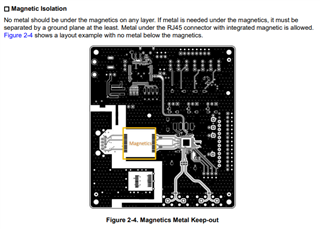
In the application report: Ethernet PHY PCB Design Layout Checklist (SNLA387), there is a section that talks about Magnetic Isolation w/ reference to Figure 2-4 on page 4.
Can you please clarify the following statement: "No metal should be under the magnetics on any layer. If metal is needed under the magnetics, it must be separated by a ground plane at the least."
Does this mean that if the design limits the ability to void all layers, should there be no void or should there be at least one gnd layer below to void?
What is the purpose of the void under the transformers?
Link and screenshot:
https://www.ti.com/lit/pdf/snla387