This thread has been locked.
If you have a related question, please click the "Ask a related question" button in the top right corner. The newly created question will be automatically linked to this question.
Hi Team,
1.
TCAN4550 cannot loop back mode issue:
In the state of protected registers enable, set the loop back mode bit of Test register (0x1010) to 1
The read register data is 0
Current status from CCCR is 0x00000218
Other protected registers are successfully written
Are there any other related settings for loop back mode that need attention?
2. Does Vio need delay? ms
Kevin,
An engineer has been notified of your post and will respond by end of business 12/14/2022 CST.
Regards,
Eric Hackett
Hello Kevin,
There are two different types of loopback that can be configured.
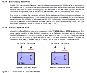
If you want the device configured for Internal Loop Back Mode, the TEST.LBCK bit (0x1010.4) should be set to '1' which enables the TX data to loop back to the RX. Also, the CCCR.MON bit (0x1018.5) should be set which disconnects the TX data from reaching the CAN bus.
However, if you clear the CCCR.MON bit, or set it to '0', this will configure the device for an External loop back mode which will allow the TX data to be output on the CAN bus as well as looped back to the RX input. The external CAN bus data will not reach the RX input in this mode. The following image is taken from the Bosch M_CAN User's Guide and is a good illustration of how the device is configured. You can find the full guide at this (Link).
The value of your CCCR register is problematic and shows bits 4 and 3 are set to '1' which indicates that a request to stop the clock has been made and acknowledged. Stopping the clock will interfere with normal operation and bit 4 should not have a '1' written to it to keep the clock running. When writing to the CCCR register, bit 4 should always be set to '0'.
Regards,
Jonathan
Hi Kevin,
No, there is no delay required. A typical use for the Inhibit (INH) pin is to connected it to the enable pin of the power regulator that supplies the MCU and VIO rail. When the board is placed in a low power sleep mode and the TCAN4550 receives a wake up pattern on the CAN bus, the INH pin will be driven High and enable the low voltage regulator, which in turn powers up the MCU and provides power to the TCAN4550 VIO pin.
This figure in the datasheet you are referencing simply states that in this situation, there will be some delay between the INH pin going High and the VIO rail ramping up. This delay will be system dependent based on the type of regulator used, the amount of capacitance on the rail, etc.
The majority of the TCAN4550 device is supplied by the VSUP pin. The VIO rail is only used to set the Digital IO levels and to power the Clock circuit. Both the VSUP and VIO rails must be active for the TCAN4550 to operate normally, but there is no power sequencing requirements in the TCAN4550 and both supplies can be ramped together, or in any sequence your application needs. However, because the VSUP is typically connected to the Battery in automotive applications, it generally is always present and only the VIO rails becomes disabled in the low power sleep mode.
Regards,
Jonathan