This thread has been locked.

If you have a related question, please click the "Ask a related question" button in the top right corner. The newly created question will be automatically linked to this question.

DS90UB954-Q1: registers settings

Part Number: DS90UB954-Q1
Other Parts Discussed in Thread: DS90UB953-Q1

hello team:
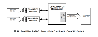
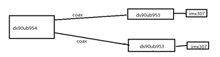
ds90ub954 is connected to two ds90ub953a,each ds90ub953a is connected to one image sensor(imx307).How to config the registers of ds90ub954 and ds90ub953 ? 

The following is our  register settings, now the sensor cannot work properly. reported cci error  . pls help to check it, thanks !

// 954
{0x01,0x04,0x00},
{0x1F,0x00,0x0}
{0x11,0x21,0x0}
{0x32,0x01,0x00},
{0x4c,0x01,0x00},
{0x58,0x5e,0x00},
{0x5c,0x30,0x00},
{0x5d,0x34,0x00},
{0x65,0x34,0x00},
{0x6d,0x7C,0x00},
{0x7C,0x00,0x00},
{0xB9,0x3F,0x00},
{0x72,0xE4,0x00}
{0x32,0x01,0x00},
{0x4c,0x12,0x00},
{0x58,0x5e,0x00},
{0x5c,0x30,0x00},
{0x5d,0x34,0x00},
{0x65,0x34,0x00},
{0x6d,0x7C,0x00},
{0x7C,0x00,0x00},
{0xB9,0x3F,0x00},
{0x72,0xE1,0x00}
{0x32,0x01,0x00},
{0x4c,0x01,0x00},
{0x58,0x00,0x00},
{0x32,0x01,0x00},
{0x4c,0x12,0x00},
{0x58,0x00,0x00},

// stream
{0x32,0x01,0x0},
{0x33,0x23,0x0},
{0x20,0x00,0x0},
{0x21,0x81,0x0}

// port 2
{0x20,0xe0,0x0},
{0x32,0x01,0x0},
{0x33,0x00,0x0}

//port 1
{0x20,0xd0,0x0},
{0x32,0x01,0x0},
{0x33,0x00,0x0}


// 953
{0x01,0x01,0x0}
{0x02,0x73,0x0}
{0x05,0x0b,0x0},
{0x33,0x00,0x0},
{0x02,0x73,0x0}
{0x0d,0xf0,0x0},
{0x0e,0x0f,0x0}

  • Hello Willywan,

    Do you have stable LOCK between DES and both SER?

    Do you have I2C communication between the DES and both SER? Between DES and both Image sensors?

    What type of error is that? And where it is reported?

    What do you mean by "the sensor cannot work properly" can you specify?

  • Hi Hamzeh:

    Thank you very much for your response immediately. Yes, I used I2C communication between the DES , both SER and both Image Sensors.   I getting error frames and the both sensors are stuck in the preview when the both sensors opened simultaneously . But open each sensor on individually, and working right.   Currently, my configurations for sensors(imx307), SER(Ti953) and DES(Ti954) as follows  :

    Sensor 1: 1920 x 1080 with 30fps

    Sensor 2: 1920 x 1080 with 30fps

    Lanecount : 4

    Datarate : 445.5Mbps/lane

    Datatype : RAW10


    // setting 953 mipi lane count.

    write(953_addr, 0x02, 0x73)  // set 4 lane


    Ti954 configurations:

    //1, set mipi and reset

    write(954_addr,0x01,0x04)   // reset chips

    write(954_addr,0x1F,0x00)  // set csi transmitter speed 1.6Gpbs

    //2, set rx port

    write(954_addr, 0x4c, 0x01)  // select port 0

    write(954_addr, 0x58, 0x5e)  // enable pass through

    write(954_addr, 0x5c, 0x30)  // set 953 alias id

    write(954_addr, 0x5d,0x34) // sensor addr

    write(954_addr, 0x65,0x34}, // sensor alias id

    write(954_addr, 0x6d,0x7c), // csi mode, coax mode

    write(954_addr, 0x72, 0xe4)  //  set virtual channel vc-id 0

    write(954_addr, 0x4c, 0x12)  // select port 1

    write(954_addr, 0x58, 0x5e) //  enable pass through

    write(954_addr, 0x5c, 0x30)  // set 953 alias id

    write(954_addr, 0x5d,0x34) // sensor addr

    write(954_addr, 0x65,0x34}, // sensor alias id

    write(954_addr, 0x6d,0x7c), // csi mode, coax mode

    write(954_addr, 0x72, 0xe1) // set virtual channel vc-id 1

    //3,  start stream

    write(954_addr, 0x20,0x00),  // enable port0 and port1

    write(954_addr,0x21,0x81),   //  enable forwarding

    write(954_addr, 0x33,0x23),  // enable csi output, continue clock,  2lane.


    what configurations have I missed except these configurations? also, above my settings whether the port1 overwrite port0 ?  please help me to check it.

    Thanks & Regards,

    Willywan

  • Hello Willywan,

    Due to the holiday break, the FPD team is out of office until the 28th. So we will resume activity on this thread at that time. Thank you for your patience

    Best Regards,

    Casey 

  • Hi  Casey:

    We are in hurry to solve this issues, which will affect the project schedule. Can you please coordinate and give priority to it? Thank you!

  • Hello Willywan,

    We will resume activity on 12/28 

    Best Regards,

    Casey 

  • Hello Willywan,

    I will review and feedback to you before the end of the day!

  • Can you provide a dump for the following 954 diagnostic registers, for both Rx ports:

    0x02-0x06, 0x1F-0x24, 0x33-0x37, 0x40-0x49, 0x4C-0x58, 0x5B-0x6D, 0x70-0x76, 0x7A-0x7C, 0xD2-0xDB.

  • Hi Hamzeh:

    Apoligize for my carelessness , I'm a rookie, I have corrected the erros for registers of 954.
    Now, I would like to enquire two new questions for our system.

    Question 1:
    How to configure the registers for combining the data from both sensors to one csi-2 output at 954 ?
    the block diagram of our system as below (8.3  System Examples, figure 51):

    I used below Initialize sequence:


    I used below Initialize sequence:

    //Sensor 0 configure VC0
    //Sensor 1 configure VC1
    write(954_addr, 0x0C, 0x83), // default, Enable both RX0 & RX1
    write(954_addr, 0x1F, 0x00), // 1.6Gbps
    write(954_addr, 0x4C, 0x01), // RX0
    write(954_addr, 0x72, 0xE4), // default, Sensor0 VC0 to CSI-TX VC0
    write(954_addr, 0x4C, 0x12), // RX1
    write(954_addr, 0x72, 0xE4), // Sensor1 VC1 to CSI-TX VC0, correct?
    write(954_addr, 0x33, 0x21), // enable CSI output & 2 lane & non continuous clock.
    write(954_addr, 0x21, 0x81), // enable csi Replicate Mode & Round Robin forwarding
    write(954_addr, 0x20, 0x00), // forwarding all RX to CSI0
    write(954_addr, 0x4C, 0x0F), // RX_PORT0 read; RX0/1 write
    write(954_addr, 0x58, 0x5E),
    write(954_addr, 0x5C, 0x30),
    write(954_addr, 0x5D, 0x34),
    write(954_addr, 0x65, 0x18),
    // 953
    write(953_addr, 0x02, 0x73) // set 4 lane

    Question 2:
    the register 0x72[1:0] at 954, how do I understand 0x72[0] and 0x72[1] bit, what means of each of bits?

    Thanks & Regards,

    Willywan

  • Hello Willywan,

    I have made some corrections:

    write(954_addr, 0x0C, 0x83), // default, Enable both RX0 & RX1
    write(954_addr, 0x1F, 0x00), // 1.6Gbps

    write(954_addr, 0x4C, 0x0F), // RX_PORT0 read; RX0/1 write
    Do not write reserved registers! For enabling RX0/1, just write: 0x03 instead of 0x0F

    write(954_addr, 0x72, 0xE4), // default, Sensor0 VC0 and Sensor1 VC1

    write(954_addr, 0x58, 0x5E),
    write(954_addr, 0x5C, 0x30),
    write(954_addr, 0x5D, 0x34),
    write(954_addr, 0x65, 0x18),

    Here you should do any SER configurations and then Image sensor configurations!

    write(954_addr, 0x33, 0x21), // enable CSI output & 2 lane & non continuous clock.
    write(954_addr, 0x21, 0x81), // enable csi Replicate Mode & Round Robin forwarding
    You should not enable replication for this case. Just write 0x21 = 0x01


    write(954_addr, 0x20, 0x00), // forwarding all RX to CSI0

    ======================

    Sensor 1: 1920 x 1080 with 30fps

    Sensor 2: 1920 x 1080 with 30fps

    Lanecount : 4

    Datarate : 445.5Mbps/lane

    Datatype : RAW10

    Are you sure the CSI-2 input datarate on each SER lane is 445.5Mbps/lane? 

  • Hi Hamzeh:

    Thank you very much for your quikly repsponse.  

    Sensor 1: 1920 x 1080 with 30fps

    Sensor 2: 1920 x 1080 with 30fps

    Lanecount : 4

    Datarate : 445.5Mbps/lane

    Datatype : RAW10

    Are you sure the CSI-2 input datarate on each SER lane is 445.5Mbps/lane? 

    Yes, as per imx307 datasheet,  445.5Mbps/lane (using 4 lane),  891Mbps/lane (using 2 lane). currently, I used 2 lane and the datarate is 891Mbps/lane for both same sensor. 

    Now, I want to combine both sensor's frame and output to CSI-2 Port 0 in 2 data lanes and 1 clock lane,  but ISP's MIPI CSI have't received proper MIPI signals.   I configured the Internal FrameSync , VC-ID mapping and  Line-Concatenate Forwarding(as below the diagram ) features, and my codes refer to 954 datasheet 7.4.28.6.1 example codes. 

    as per datasheet of 954,I rewrite the registers initlialize sequeue. as follows:  

    {U954,0x4c,0x01}, // RX0
    {U954,0x58,0x5e}, // i2c passthrough
    {U954,0x6f,0xaa}, // BC_GPIO_CTL, [7:4]set BC GPIO2/GIO3 FrameSync signal
    {U954,0x5c,0x30}, // SER_ALIAS_ID
    {U954,0x5d,0x34}, // SlaveID[0]
    {U954,0x65,0x18}, // Sensor0 slaveaddr
    {U954,0x6d,0x7c}, // enable CSI Mode, Coax mode
    {U954,0x72,0xE4}, // Sensor0 VC0 to CSI-TX VC0 (CSI-2 input mode)

    {U954,0x4c,0x12}, // RX1
    {U954,0x58,0x5e}, // i2c passthrough
    {U954,0x6f,0xaa}, // BC_GPIO_CTL1, set BC GPIO2/GPIO3 FrameSync signal
    {U954,0x5c,0x30}, // SER_ALIAS_ID
    {U954,0x5d,0x34}, // SlaveID[0]
    {U954,0x65,0x20}, // Sensor1 slaveaddr
    {U954,0x6d,0x7c}, // enable CSI Mode, Coax mode
    {U954,0x72,0xE4}, // Sensor1 VC0 to CSI-TX VC0 (CSI-2 input mode)

    {U954,0x12,0x91}, // enable gpio2 output
    {U954,0x19,0x0a}, 
    {U954,0x1a,0xd7},
    {U954,0x1b,0x61},
    {U954,0x1c,0xa0},
    {U954,0x18,0x01}, // FS_CTL,Enable internal Gen Fsync

    {U954,0x33,0x23}, // CSI EN & Cont Clock Enable, 2 lane
    {U954,0x20,0x00}, // forwarding all RX to CSI0
    {U954,0x21,0x0c}, // Synchronous forwarding with line concatenation.

    //953
    {U953,0x0d,0xf0}, // Enable remote gpio0~gpio3
    {U953,0x0e,0xf0} // Enable gpio0~gpio3 output

    Thanks,

    Willywan

  • Willywan,

    The DS90UB953-Q1 has a maximum CSI-2 lane rate of 800Mbps/lane when using 25MHz REFCLK on the 954 or 832Mbps/lane when using a 26MHz REFCLK on 954. There is no way to support 891Mbps/lane speed, so that is likely your issue here

    Best Regards,

    Casey 

  • Hi Casey,

    Iconfiguring sensor‘s CSI-2  to 4 Lane(445.5Mbps/Lane) , 953 to 4 lane(800Mbps/Lane, 25MHz REFCLK ), and 954 to 4 lane(1.6Gbps/Lane), Is that right?

    I want to combine both sensor's data to CSI-2 port0, How to configure registers and initialize sequeue?

    {U954,0x4c,0x01}, // RX0
    {U954,0x58,0x5e}, // i2c passthrough
    {U954,0x6f,0xaa}, // BC_GPIO_CTL, [7:4]set BC GPIO2/GIO3 FrameSync signal
    {U954,0x5c,0x30}, // SER_ALIAS_ID
    {U954,0x5d,0x34}, // SlaveID[0]
    {U954,0x65,0x18}, // Sensor0 slaveaddr
    {U954,0x6d,0x7c}, // enable CSI Mode, Coax mode
    {U954,0x72,0xE4}, // Sensor0 VC0 to CSI-TX VC0 (CSI-2 input mode)

    {U954,0x4c,0x12}, // RX1
    {U954,0x58,0x5e}, // i2c passthrough
    {U954,0x6f,0xaa}, // BC_GPIO_CTL1, set BC GPIO2/GPIO3 FrameSync signal
    {U954,0x5c,0x30}, // SER_ALIAS_ID
    {U954,0x5d,0x34}, // SlaveID[0]
    {U954,0x65,0x20}, // Sensor1 slaveaddr
    {U954,0x6d,0x7c}, // enable CSI Mode, Coax mode
    {U954,0x72,0xE4}, // Sensor1 VC0 to CSI-TX VC0 (CSI-2 input mode)

    {U954,0x12,0x91}, // enable gpio2 output
    {U954,0x19,0x0a}, 
    {U954,0x1a,0xd7},
    {U954,0x1b,0x61},
    {U954,0x1c,0xa0},
    {U954,0x18,0x01}, // FS_CTL,Enable internal Gen Fsync

    {U954,0x33,0x23}, // CSI EN & Cont Clock Enable, 2 lane
    {U954,0x20,0x00}, // forwarding all RX to CSI0
    {U954,0x21,0x0c}, // Synchronous forwarding with line concatenation.

    //953
    {U953,0x0d,0xf0}, // Enable remote gpio0~gpio3
    {U953,0x0e,0xf0} // Enable gpio0~gpio3 output

    ====================================================================

    // 953  registers

    {U953,0X01,0X01}, // reset
    {U953,0X05,0X08}, // 48.4 MHz to 51 MHz, set for 4 Gbps line rate mode
    {U953,0X33,0X00}, // GPIOs disabled
    {U953,0X02,0X73} // 4 lane
    {U953,0x0d,0xf0}, // remote gpios
    {U953,0x0e,0xf0} // gpio output

    above register configurations whether are correct on 954 and 953? 

    Thanks & Regards,

    Willywan

  • Hello Willywan,

    Due to the US federal holiday, our team is currently out of office and will return tomorrow 1/2/23. Thank you for your patience 

    Best Regards,

    Casey

  • Hello Casey,

    Thank you very much for your repsponse. I would like to equire two questions:

    question1:

    I have't get the image after merged for both sensors when using above initialization sequeue. it seems that the rx1 port have't recieved frame sync signal. I refer to the codes of sections of datasheet's 7.4.27.2.1.

    below is the update initialization sequeue:

    //SET PORT

    {UB954, 0x4c,0x01}, // RX0

    {UB954, 0x72,0xe4}, // Sensor0 VC0 to CSI-TX VC0 (CSI-2 input mode)

    {UB954, 0x4c,0x12}, // RX1

    {UB954, 0x72,0xe1}, // Sensor1 VC0 to CSI-TX VC1 (CSI-2 input mode)

    {UB954, 0x4c,0x03}, // broadcast write to Rx Port 0 and Rx Port 1, Rx0 read.

    {UB954, 0x58,0x5d}, // i2c passthrough, BC_ALWAYS_ON, BC_FREQ_SEELCT:50Mbps

    {UB954, 0x5c,0x30}, // SER_ALIAS_ID

    {UB954, 0x5d,0x34}, // SlaveID[0], both sensor have same slave addr and vc 0

    {UB954, 0x65,0x34}, // Sensor slaveaddr

    {UB954, 0x6d,0x7c}, // coax mode, csi mode

    {UB954, 0x7C,0x01}

    // SET FRAME SYNC

     // 30fps, approximately 55556(1/30/600ns) frame periods for 50Mbps BC

     {UB954, 0x4c,0x01}, // RX0

     {UB954, 0x58,0x5e}, // i2c passthrough, BC_ALWAYS_ON, BC_FREQ_SEELCT:50Mbps

     {UB954, 0x6f,0x8a}, // BC_GPIO_CTL, BC GPIO Control: Link BC GPIO2 to be Frame Sync output

     {UB954, 0x4c,0x12}, // RX1

     {UB954, 0x58,0x5e}, // i2c passthrough, BC_ALWAYS_ON, BC_FREQ_SEELCT:50Mbps

     {UB954, 0x6f,0x8a}, // BC_GPIO_CTL, BC GPIO Control: Link BC GPIO2 to be Frame Sync output

     {UB954, 0x12,0x91}, // GPIO2 FrameSync signal; Device Status; Enabled

     {UB954, 0x19,0x15}, // FS_HIGH_TIME1: 10% duty cycle. 30Hz

     {UB954, 0x1a,0xb3}, // FS_HIGH_TIME0: Create an aproximate 30Hz square wave for Frame Sync

     {UB954, 0x1b,0xc3}, // FS_LOW_TIME1

     {UB954, 0x1c,0x4f}, // FS_LOW_TIME0

     {UB954, 0x18,0x01}, // FS_CTL,Enable internal Gen Fsync from port0

     {UB954, 0x33,0x21}, // CSI ENABLE & Cont Clock Enable, 2Lane.

     {UB954, 0x21,0x0c}, // Synchronous forwarding with line concatenation.

     {UB954, 0x20,0x00}, // forwarding all RX to CSI0

    {UB953, 0x05,0x0b},  // no sync

    {UB953, 0x33,0x00},

    {UB953, 0x02,0x73},// set 4 lane

    {UB953, 0x0d,0x40}, // Enable remote des GPIO2 data on local GPIO

    {UB953, 0x0e,0x40} // Enable GPIO2 ouput

    But, I got the value of register's status as follows:

    {0x4d, 0x3}
    {0x4e, 0xc}
    {0x55, 0x0}
    {0x56, 0x0}
    {0x4f, 0x64}
    {0xe, 0x0}
    {0x4, 0xdf}
    {0x72, 0xe4}
    {0x73, 0x4}
    {0x74, 0x44}
    {0x75, 0xb}
    {0x76, 0x40}
    {0x22, 0x0}
    {0x35, 0x1}

    pls help check it.

    I double checked the datasheet of sensors again.  updated both sensor's  csi lane count to 2(datarate: 445.5Mbps/Lane, 1920*1080@30fps),  953 : 4 lane and 954: 2 lane(800Mbps/Lane, output size: 3840*1080)

    question2:

    we use the length 15cm of coax line, the single sensor work normally. But using length 300cm of coax line, the single sensor doesn't work normally, it report "I2C NACK" errors. what is the reason for this ?

    Thanks & Regards,

    Willywan

  • Hello,

    Let me go through these and get back to you!

  • Hello Hamzeh,

    Is there any feedback? I was able to measure frame sync signals from gpio2 on both 953s, but the images did not combined on 954,why?

  • Hello Willywan,

    If you want to combine both images on the 954, you should use one of the synchronized Forwarding modes, such as Basic Synchronized forwarding, Line-Interleave forwarding or Line-Concatenated forwarding. Please refer to datasheet section "7.4.28.3 Synchronized Forwarding"

  • Hello Hamzeh,

    I refer to datasheet section 7.4.28.3, I used Line-Concatenated forwarding mode, but I was able to saw the images from RX0 on 954, I can’t saw the any images from RX1, the 0x73~0x76 haved image data from RX1,please check my register’s settings whether is all correct. Thanks!

    Regards,

    Willywan.

  • Hello Willywan,

    Which Mode are you using on the DES and on both SER? Is this Back channel Synchrunuons Mode or External Clock mode?
    I can see in 954 reg 0x58=0x5D that you are using BC 25 Mbps which is too low for your system. You should use 0x5E if Synch Mode and 0x5A if Non-Synch Mode.
    Then you are changing that again to 0x5E!! Any reason for switching?

    I double checked the datasheet of sensors again.  updated both sensor's  csi lane count to 2(datarate: 445.5Mbps/Lane, 1920*1080@30fps),  953 : 4 lane and 954: 2 lane(800Mbps/Lane, output size: 3840*1080)

    Let me summarize my understanding and please correct me if I am wrong!

    You are using 2 Cameras with UB953. Each UB953 is setup to use 2x CSI-2 lanes at ~445Mbps/lane.

    The UB954 is using 2x CSI-2 lanes at speed of 800Mbps/lane. Is that correct? Because I am confused, above you are saying some time 2x lanes and other time 4x lanes!! Also, some time you said 800Mbps/lane and other time 1.6Gbps/lane!! Please clarify!

    we use the length 15cm of coax line, the single sensor work normally. But using length 300cm of coax line, the single sensor doesn't work normally, it report "I2C NACK" errors. what is the reason for this ?

    If you are seeing errors at longer cable that means you have higher insertion loss and signal attenuation. Which means your Hardware design layout and/or cable type/ connector type is not good enough, or your PoC Filter design is not impedance matched!


  • Hello Hamzeh,

    Thank you very much for your repsponse. your understand is currect. I aplogize for above my inaccurate descriptions.  this issure has resolved.

    Thanks & Regards,

    Willywan.

  • Hello Willywan,

    as discussed on the call, here are the details:

    I need reg dumps from SER and DES showing this behavior.
    I need Data type, Frame rate, Number of bits per second, Horizontal and vertical resolution from each image sensor.

    I need schematic from SER and from DES.


    ---------
    To make sure your link is good enough, you need to measure Insertion loss and return loss.
    or test using MAP Tool
    ---------
    Attached you can find our Channel specs for ADAS
    ---------
    schematic from 953 and from 954. I need to check this to see which MODE is used. If you rae using 2.5Mbps back channel, then 953 will work in backward Mode and no CLKOUT will be provided to image sensor.
    ---------
    LOCK time is typically 20ms.
    Max LOCK time for RAW mode is 200ms, and for CSI mode is 300ms.
    ---------
    System Initialization sequence:
    1) Initialize DES
    2) wait for stable LCOK
    3) Initialize SER
    4) Initialize Image sensor
    5) Wait ~30 ms
    6) enable CSI-2 port
    7) enable CSI-2 forwarding
    -----------

    FPD-Link III Channel-Requirements -ADAS chipsets-Rev0p81.pdf

  • Hello Hamzeh,

    Schematic diagram of 953 and 954, and the  table of registers configuration sequence has been emailed. Currently, we are investigating the frame loss problem, can you give some advice? 

  • Yes, I will review and get back to you soon.

  • Hello Willywan,

    From the schematic review I have the following feedback:

    953:
    - Not clear how your PDB is controlled! Also, not clear if you maintain the power-up sequence or not!
    - Using Non-Synchronous Mode but not connecting the External Oscillator to the 953.
    - When using Non-Sync Mode, it is recommended to use 22uH or 33uH inductor instead of the 10uH on PoC filter(L1)
    - Not clear which FB are used on the PoC!

    954:
    - On MODE pin you are using 10K and 12K resistors which is slightly different than our recommendation. If your 1.8V is above than average, then the target voltage will be above our allowed limits.
    - On VDD18_CSI a 10uF capacitor is missing.
    - It looks like the FB used on the PoC are not sufficient. These shall have 1.5Kohm impedance!

    ---------------

    Also, from the schematic it looks like the SER is set to Non-Synchronous Mode but not connected to the External Oscillator! At the same time, the DES is setup to run in Sync mode. Please use the same Mode on both devices!!

    --------------

    I did not find any registers dump in the attached folders. Also, the provide layout screen shot is not sufficient for review. Please provide Gerber files. The one provided in the ppt can't be opened!

  • Dear TI:

                  Please refer to the attached reply

                  Meigsmart_DS90UB953_4_Case_reply(230114).pptxMT564_MB_V1.00_GERBER(221129).rar

  • Hello HemZeh,

    I'm sorry for my delayed replying. following is our registers dump of 954 and 953's. please check it. Thanks. 

    // rx0 dump
    {0x0,0x60}
    {0x1,0x0}
    {0x2,0x1e}
    {0x3,0x20}
    {0x4,0xdf}
    {0x5,0x1}
    {0x6,0x0}
    {0x7,0xfe}
    {0x8,0x1c}
    {0x9,0x10}
    
    {0xa,0x7a}
    {0xb,0x7a}
    {0xc,0xbf}
    {0xd,0x9}
    {0xe,0x0}
    {0xf,0x7f}
    {0x10,0x0}
    {0x11,0x0}
    {0x12,0x0}
    {0x13,0x0}
    
    {0x14,0x0}
    {0x15,0x0}
    {0x16,0x0}
    {0x17,0x0}
    {0x18,0x0}
    {0x19,0x0}
    {0x1a,0x0}
    {0x1b,0x0}
    {0x1c,0x0}
    {0x1d,0x0}
    
    {0x1e,0x4}
    {0x1f,0x0}
    {0x20,0x20}
    {0x21,0x81}
    {0x22,0x0}
    {0x23,0x0}
    {0x24,0x0}
    {0x25,0x0}
    {0x26,0x0}
    {0x27,0x0}
    
    {0x28,0x0}
    {0x29,0x0}
    {0x2a,0x0}
    {0x2b,0x0}
    {0x2c,0x0}
    {0x2d,0x0}
    {0x2e,0x0}
    {0x2f,0x0}
    {0x30,0x0}
    {0x31,0x0}
    {0x32,0x0}
    {0x33,0x21}
    {0x34,0x40}
    {0x35,0x1}
    {0x36,0x0}
    {0x37,0x0}
    {0x38,0x0}
    {0x39,0x0}
    {0x3a,0x0}
    {0x3b,0x1}
    
    {0x3c,0x14}
    {0x3d,0x6f}
    {0x3e,0x0}
    {0x3f,0x40}
    {0x40,0x0}
    {0x41,0xa7}
    {0x42,0x71}
    {0x43,0x1}
    {0x44,0x0}
    {0x45,0x0}
    
    {0x46,0x0}
    {0x47,0x0}
    {0x48,0x0}
    {0x49,0x0}
    {0x4a,0x0}
    {0x4b,0x12}
    {0x4c,0x1}
    {0x4d,0x3}
    {0x4e,0x4}
    {0x4f,0x64}
    
    {0x50,0x0}
    {0x51,0x0}
    {0x52,0x0}
    {0x53,0x3}
    {0x54,0x2}
    {0x55,0x0}
    {0x56,0x0}
    {0x57,0x0}
    {0x58,0x0}
    {0x59,0x0}
    
    {0x5a,0x0}
    {0x5b,0x30}
    {0x5c,0x30}
    {0x5d,0x34}
    {0x5e,0x0}
    {0x5f,0x0}
    {0x60,0x0}
    {0x61,0x0}
    {0x62,0x0}
    {0x63,0x0}
    
    {0x64,0x0}
    {0x65,0x18}
    {0x66,0x0}
    {0x67,0x0}
    {0x68,0x0}
    {0x69,0x0}
    {0x6a,0x0}
    {0x6b,0x0}
    {0x6c,0x0}
    {0x6d,0x7c}
    
    {0x6e,0x88}
    {0x6f,0x88}
    {0x70,0x2b}
    {0x71,0x2c}
    {0x72,0xe4}
    {0x73,0x4}
    {0x74,0x44}
    {0x75,0xb}
    {0x76,0x40}
    {0x77,0xc5}
    {0x78,0x0}
    {0x79,0x1}
    {0x7a,0x0}
    {0x7b,0x0}
    {0x7c,0x0}
    {0x7d,0x0}
    {0x7e,0x0}
    {0x7f,0x0}
    {0x80,0x0}
    {0x81,0x0}
    
    {0x82,0x0}
    {0x83,0x0}
    {0x84,0x0}
    {0x85,0x0}
    {0x86,0x0}
    {0x87,0x0}
    {0x88,0x0}
    {0x89,0x0}
    {0x8a,0x0}
    {0x8b,0x0}
    
    {0x8c,0x0}
    {0x8d,0x0}
    {0x8e,0x0}
    {0x8f,0x0}
    {0x90,0x0}
    {0x91,0x0}
    {0x92,0x0}
    {0x93,0x0}
    {0x94,0x0}
    {0x95,0x0}
    
    {0x96,0x0}
    {0x97,0x0}
    {0x98,0x0}
    {0x99,0x0}
    {0x9a,0x0}
    {0x9b,0x0}
    {0x9c,0x0}
    {0x9d,0x0}
    {0x9e,0x0}
    {0x9f,0x0}
    
    {0xa0,0x2}
    {0xa1,0xf}
    {0xa2,0x0}
    {0xa3,0x0}
    {0xa4,0x8}
    {0xa5,0x19}
    {0xa6,0x0}
    {0xa7,0x0}
    {0xa8,0x0}
    {0xa9,0x0}
    
    {0xaa,0x0}
    {0xab,0x0}
    {0xac,0x0}
    {0xad,0x0}
    {0xae,0x0}
    {0xaf,0x0}
    {0xb0,0x8}
    {0xb1,0x14}
    {0xb2,0x3f}
    {0xb3,0x8}
    
    {0xb4,0x25}
    {0xb5,0x0}
    {0xb6,0x18}
    {0xb7,0x0}
    {0xb8,0x8c}
    {0xb9,0x3f}
    {0xba,0x83}
    {0xbb,0x74}
    {0xbc,0x80}
    {0xbd,0x0}
    
    {0xbe,0x0}
    {0xbf,0x0}
    {0xc0,0x0}
    {0xc1,0x0}
    {0xc2,0x0}
    {0xc3,0x0}
    {0xc4,0x0}
    {0xc5,0x0}
    {0xc6,0x0}
    {0xc7,0x0}
    
    {0xc8,0x0}
    {0xc9,0x0}
    {0xca,0x0}
    {0xcb,0x0}
    {0xcc,0x0}
    {0xcd,0x0}
    {0xce,0x0}
    {0xcf,0x0}
    {0xd0,0x0}
    {0xd1,0x43}
    
    {0xd2,0x94}
    {0xd3,0x2}
    {0xd4,0x60}
    {0xd5,0xf2}
    //rx1 dump
    {0x0,0x60}
    {0x1,0x0}
    {0x2,0x1e}
    {0x3,0x20}
    {0x4,0xdf}
    {0x5,0x1}
    {0x6,0x0}
    {0x7,0xfe}
    {0x8,0x1c}
    {0x9,0x10}
    {0xa,0x7a}
    {0xb,0x7a}
    {0xc,0xbf}
    {0xd,0x9}
    {0xe,0x0}
    {0xf,0x7f}
    {0x10,0x0}
    {0x11,0x0}
    {0x12,0x0}
    {0x13,0x0}
    {0x14,0x0}
    {0x15,0x0}
    {0x16,0x0}
    {0x17,0x0}
    {0x18,0x0}
    {0x19,0x0}
    {0x1a,0x0}
    {0x1b,0x0}
    {0x1c,0x0}
    {0x1d,0x0}
    {0x1e,0x4}
    {0x1f,0x0}
    {0x20,0x20}
    {0x21,0x81}
    {0x22,0x0}
    {0x23,0x0}
    {0x24,0x0}
    {0x25,0x0}
    {0x26,0x0}
    {0x27,0x0}
    {0x28,0x0}
    {0x29,0x0}
    {0x2a,0x0}
    {0x2b,0x0}
    {0x2c,0x0}
    {0x2d,0x0}
    {0x2e,0x0}
    {0x2f,0x0}
    {0x30,0x0}
    {0x31,0x0}
    {0x32,0x0}
    {0x33,0x21}
    {0x34,0x40}
    {0x35,0x1}
    {0x36,0x0}
    {0x37,0x0}
    {0x38,0x0}
    {0x39,0x0}
    {0x3a,0x0}
    {0x3b,0x1}
    {0x3c,0x14}
    {0x3d,0x6f}
    {0x3e,0x0}
    {0x3f,0x40}
    {0x40,0x0}
    {0x41,0xa7}
    {0x42,0x71}
    {0x43,0x1}
    {0x44,0x0}
    {0x45,0x0}
    {0x46,0x0}
    {0x47,0x0}
    {0x48,0x0}
    {0x49,0x0}
    {0x4a,0x0}
    {0x4b,0x12}
    {0x4c,0x12}
    {0x4d,0x43}
    {0x4e,0x4}
    {0x4f,0x64}
    {0x50,0x0}
    {0x51,0x0}
    {0x52,0x0}
    {0x53,0x4}
    {0x54,0x2}
    {0x55,0x0}
    {0x56,0x0}
    {0x57,0x0}
    {0x58,0x5a}
    {0x59,0x0}
    {0x5a,0x0}
    {0x5b,0x30}
    {0x5c,0x30}
    {0x5d,0x34}
    {0x5e,0x0}
    {0x5f,0x0}
    {0x60,0x0}
    {0x61,0x0}
    {0x62,0x0}
    {0x63,0x0}
    {0x64,0x0}
    {0x,0x20}
    {0x66,0x0}
    {0x67,0x0}
    {0x68,0x0}
    {0x69,0x0}
    {0x6a,0x0}
    {0x6b,0x0}
    {0x6c,0x0}
    {0x6d,0x7c}
    {0x6e,0x88}
    {0x6f,0x88}
    {0x70,0x6b}
    {0x71,0x6c}
    {0x72,0xe1}
    {0x73,0x4}
    {0x74,0x44}
    {0x75,0xb}
    {0x76,0x40}
    {0x77,0xc5}
    {0x78,0x0}
    {0x79,0x1}
    {0x7a,0x0}
    {0x7b,0x0}
    {0x7c,0x0}
    {0x7d,0x0}
    {0x7e,0x0}
    {0x7f,0x0}
    {0x80,0x0}
    {0x81,0x0}
    {0x82,0x0}
    {0x83,0x0}
    {0x84,0x0}
    {0x85,0x0}
    {0x86,0x0}
    {0x87,0x0}
    {0x88,0x0}
    {0x89,0x0}
    {0x8a,0x0}
    {0x8b,0x0}
    {0x8c,0x0}
    {0x8d,0x0}
    {0x8e,0x0}
    {0x8f,0x0}
    {0x90,0x0}
    {0x91,0x0}
    {0x92,0x0}
    {0x93,0x0}
    {0x94,0x0}
    {0x95,0x0}
    {0x96,0x0}
    {0x97,0x0}
    {0x98,0x0}
    {0x99,0x0}
    {0x9a,0x0}
    {0x9b,0x0}
    {0x9c,0x0}
    {0x9d,0x0}
    {0x9e,0x0}
    {0x9f,0x0}
    {0xa0,0x2}
    {0xa1,0xf}
    {0xa2,0x0}
    {0xa3,0x0}
    {0xa4,0x8}
    {0xa5,0x19}
    {0xa6,0x0}
    {0xa7,0x0}
    {0xa8,0x0}
    {0xa9,0x0}
    {0xaa,0x0}
    {0xab,0x0}
    {0xac,0x0}
    {0xad,0x0}
    {0xae,0x0}
    {0xaf,0x0}
    {0xb0,0x8}
    {0xb1,0x14}
    {0xb2,0x3f}
    {0xb3,0x8}
    {0xb4,0x25}
    {0xb5,0x0}
    {0xb6,0x18}
    {0xb7,0x0}
    {0xb8,0x8c}
    {0xb9,0x3f}
    {0xba,0x83}
    {0xbb,0x74}
    {0xbc,0x80}
    {0xbd,0x0}
    {0xbe,0x0}
    {0xbf,0x0}
    1{0xc0,0x0}
    {0xc1,0x0}
    {0xc2,0x0}
    {0xc3,0x0}
    {0xc4,0x0}
    {0xc5,0x0}
    {0xc6,0x0}
    {0xc7,0x0}
    {0xc8,0x0}
    {0xc9,0x0}
    {0xca,0x0}
    {0xcb,0x0}
    {0xcc,0x0}
    {0xcd,0x0}
    {0xce,0x0}
    {0xcf,0x0}
    {0xd0,0x0}
    {0xd1,0x43}
    {0xd2,0x94}
    {0xd3,0x2}
    {0xd4,0x60}
    {0xd5,0xf2}
    {0x0,0x60}
    {0x1,0x0}
    {0x2,0x1e}
    {0x3,0x20}
    {0x4,0xdf}
    {0x5,0x1}
    {0x6,0x0}
    {0x7,0xfe}
    {0x8,0x1c}
    {0x9,0x10}
    {0xa,0x7a}
    {0xb,0x7a}
    {0xc,0xbf}
    {0xd,0x9}
    {0xe,0x0}
    {0xf,0x7f}
    {0x10,0x0}
    {0x11,0x0}
    {0x12,0x0}
    {0x13,0x0}
    {0x14,0x0}
    {0x15,0x0}
    {0x16,0x0}
    {0x17,0x0}
    {0x18,0x0}
    {0x19,0x0}
    {0x1a,0x0}
    {0x1b,0x0}
    {0x1c,0x0}
    {0x1d,0x0}
    {0x1e,0x4}
    {0x1f,0x0}
    {0x20,0x20}
    {0x21,0x81}
    {0x22,0x0}
    {0x23,0x0}
    {0x24,0x0}
    {0x25,0x0}
    {0x26,0x0}
    {0x27,0x0}
    {0x28,0x0}
    {0x29,0x0}
    {0x2a,0x0}
    {0x2b,0x0}
    {0x2c,0x0}
    {0x2d,0x0}
    {0x2e,0x0}
    {0x2f,0x0}
    {0x30,0x0}
    {0x31,0x0}
    {0x32,0x0}
    {0x33,0x21}
    {0x34,0x40}
    {0x35,0x1}
    {0x36,0x0}
    {0x37,0x0}
    {0x38,0x0}
    {0x39,0x0}
    {0x3a,0x0}
    {0x3b,0x1}
    {0x3c,0x14}
    {0x3d,0x6f}
    {0x3e,0x0}
    {0x3f,0x40}
    {0x40,0x0}
    {0x41,0xa7}
    {0x42,0x71}
    {0x43,0x1}
    {0x44,0x0}
    {0x45,0x0}
    {0x46,0x0}
    {0x47,0x0}
    {0x48,0x0}
    {0x49,0x0}
    {0x4a,0x0}
    {0x4b,0x12}
    {0x4c,0x12}
    {0x4d,0x43}
    {0x4e,0x4}
    {0x4f,0x64}
    {0x50,0x0}
    {0x51,0x0}
    {0x52,0x0}
    {0x53,0x4}
    {0x54,0x2}
    {0x55,0x0}
    {0x56,0x0}
    {0x57,0x0}
    {0x58,0x5a}
    {0x59,0x0}
    {0x5a,0x0}
    {0x5b,0x30}
    {0x5c,0x30}
    {0x5d,0x34}
    {0x5e,0x0}
    {0x5f,0x0}
    {0x60,0x0}
    {0x61,0x0}
    {0x62,0x0}
    {0x63,0x0}
    {0x64,0x0}
    {0x,0x20}
    {0x66,0x0}
    {0x67,0x0}
    {0x68,0x0}
    {0x69,0x0}
    {0x6a,0x0}
    {0x6b,0x0}
    {0x6c,0x0}
    {0x6d,0x7c}
    {0x6e,0x88}
    {0x6f,0x88}
    {0x70,0x6b}
    {0x71,0x6c}
    {0x72,0xe1}
    {0x73,0x4}
    {0x74,0x44}
    {0x75,0xb}
    {0x76,0x40}
    {0x77,0xc5}
    {0x78,0x0}
    {0x79,0x1}
    {0x7a,0x0}
    {0x7b,0x0}
    {0x7c,0x0}
    {0x7d,0x0}
    {0x7e,0x0}
    {0x7f,0x0}
    {0x80,0x0}
    {0x81,0x0}
    {0x82,0x0}
    {0x83,0x0}
    {0x84,0x0}
    {0x85,0x0}
    {0x86,0x0}
    {0x87,0x0}
    {0x88,0x0}
    {0x89,0x0}
    {0x8a,0x0}
    {0x8b,0x0}
    {0x8c,0x0}
    {0x8d,0x0}
    {0x8e,0x0}
    {0x8f,0x0}
    {0x90,0x0}
    {0x91,0x0}
    {0x92,0x0}
    {0x93,0x0}
    {0x94,0x0}
    {0x95,0x0}
    {0x96,0x0}
    {0x97,0x0}
    {0x98,0x0}
    {0x99,0x0}
    {0x9a,0x0}
    {0x9b,0x0}
    {0x9c,0x0}
    {0x9d,0x0}
    {0x9e,0x0}
    {0x9f,0x0}
    {0xa0,0x2}
    {0xa1,0xf}
    {0xa2,0x0}
    {0xa3,0x0}
    {0xa4,0x8}
    {0xa5,0x19}
    {0xa6,0x0}
    {0xa7,0x0}
    {0xa8,0x0}
    {0xa9,0x0}
    {0xaa,0x0}
    {0xab,0x0}
    {0xac,0x0}
    {0xad,0x0}
    {0xae,0x0}
    {0xaf,0x0}
    {0xb0,0x8}
    {0xb1,0x14}
    {0xb2,0x3f}
    {0xb3,0x8}
    {0xb4,0x25}
    {0xb5,0x0}
    {0xb6,0x18}
    {0xb7,0x0}
    {0xb8,0x8c}
    {0xb9,0x3f}
    {0xba,0x83}
    {0xbb,0x74}
    {0xbc,0x80}
    {0xbd,0x0}
    {0xbe,0x0}
    {0xbf,0x0}
    {0xc0,0x0}
    {0xc1,0x0}
    {0xc2,0x0}
    {0xc3,0x0}
    {0xc4,0x0}
    {0xc5,0x0}
    {0xc6,0x0}
    {0xc7,0x0}
    {0xc8,0x0}
    {0xc9,0x0}
    {0xca,0x0}
    {0xcb,0x0}
    {0xcc,0x0}
    {0xcd,0x0}
    {0xce,0x0}
    {0xcf,0x0}
    {0xd0,0x0}
    {0xd1,0x43}
    {0xd2,0x94}
    {0xd3,0x2}
    {0xd4,0x60}
    {0xd5,0xf2}

    // 953 dump
    {0x0, 0x30}
    {0x1, 0x0}
    {0x2, 0x73}
    {0x3, 0x4a}
    {0x4, 0x0}
    {0x5, 0x0}
    {0x6, 0x49}
    {0x7, 0xf2}
    {0x8, 0xfe}
    {0x9, 0x1e}
    {0xa, 0x10}
    {0xb, 0x7f}
    {0xc, 0x7f}
    {0xd, 0x40}
    {0xe, 0x40}
    {0xf, 0x0}
    {0x10, 0x0}
    {0x11, 0x0}
    {0x12, 0x0}
    {0x13, 0x0}
    {0x14, 0x0}
    {0x15, 0x20}
    {0x16, 0x18}
    {0x17, 0x3c}
    {0x18, 0x80}
    {0x19, 0x62}
    {0x1a, 0x62}
    {0x1b, 0x62}
    {0x1c, 0x0}
    {0x1d, 0x0}
    {0x1e, 0x0}
    {0x1f, 0x0}
    {0x20, 0x0}
    {0x21, 0x0}
    {0x22, 0x0}
    {0x23, 0x0}
    {0x24, 0x0}
    {0x25, 0x2}
    {0x26, 0x0}
    {0x27, 0x0}
    {0x28, 0x67}
    {0x29, 0x33}
    {0x2a, 0x1}
    {0x2b, 0x0}
    {0x2c, 0x0}
    {0x2d, 0x0}
    {0x2e, 0x0}
    {0x2f, 0x0}
    {0x30, 0x0}
    {0x31, 0x20}
    {0x32, 0x9}
    {0x33, 0x0}
    {0x34, 0x0}
    {0x35, 0x11}
    {0x36, 0x0}
    {0x37, 0x60}
    {0x38, 0x0}
    {0x39, 0x0}
    {0x3a, 0x0}
    {0x3b, 0x0}
    {0x3c, 0x0}
    {0x3d, 0x0}
    {0x3e, 0x0}
    {0x3f, 0x0}
    {0x40, 0x0}
    {0x41, 0x0}
    {0x42, 0x0}
    {0x43, 0x0}
    {0x44, 0x0}
    {0x45, 0x0}
    {0x46, 0x0}
    {0x47, 0x0}
    {0x48, 0x0}
    {0x49, 0x0}
    {0x4a, 0x0}
    {0x4c, 0x0}
    {0x4d, 0x0}
    {0x4e, 0x0}
    {0x4f, 0x0}
    {0x50, 0x20}
    {0x51, 0xc0}
    {0x52, 0x57}
    {0x53, 0x0}
    {0x54, 0x0}
    {0x55, 0xff}
    {0x56, 0xff}
    {0x57, 0x0}
    {0x58, 0x7}
    {0x59, 0x7}
    {0x5a, 0x7}
    {0x5b, 0x0}
    {0x5c, 0x0}
    {0x5d, 0x0}
    {0x5e, 0x0}
    {0x5f, 0x0}
    {0x60, 0x0}
    {0x61, 0x12}
    {0x62, 0x80}
    {0x63, 0x1}

  • Hello Willywan,

    We are currently OoO due to the public US holiday and will return to this thread on 1/17. Thank you for your patience. 

    Best Regards,

    Casey 

  • Dear  Hemzeh:

    I'm Ricky in charge of hardware. I have two questions to answer. Thank you               

    Question 1: When the chip is started, the LOCK signal is unstable. The waveform is as follows. Is it normal?

    Question 2: Measure CSI eye map, DATA LANE| Δ VOD | has reached 20mV, exceeding 14mV of Spec, can the software be adjusted?

  • Hello Willywan,

    Question 1: When the chip is started, the LOCK signal is unstable. The waveform is as follows. Is it normal?

    No, it is not normal to lose LOCK several seconds after initial LOCK. This may indicate a marginality in the link quality between SER/DES, or there could be another type of systematic event (power supply glitch, cable disconnect, etc.) causing this

    Question 2: Measure CSI eye map, DATA LANE| Δ VOD | has reached 20mV, exceeding 14mV of Spec, can the software be adjusted?

    This is not something adjustable by registers. Can you share the report that you are referencing here? We have validated that 954 can pass the MIPI DPHY CTS without any failures, so I would suspect that this is either due to a misconfiguration, an error in the test methodology, or a PCB routing issue 

    Best Regards,

    Casey 

  • Hello Hamzeh,

    Currently, I have a problem. opening the sensor of 953, ISP mipi reports the errors as following.

     ERROR_CRC CPHY: Long pkt payload CRC mismatch
     CSID: 2 Error IRQ Count:1
    CSID:2 ERROR_ECC: Dphy pkt hdr errors unrecoverable

    The both 953s no frame sync,  what is the cause of this ?  Is there something wrong with my configuration?  reading the value of register 0x4d= 0x13,0x4e=0x2c. what's reason for the lock instability? 

  • Hi Willywan,

    Can you help summarize current state of issues? There has been several results reported in parallel (lock issues, CSI issues, etc). So it is difficult to understand current status of problem and where to focus.

    Hamzeh had also pointed out several things to check within schematic that could be improved.

    Regards,

    Logan

  • Hello Logan,

    sorry for my delayed replying due to our holiday. currently,  the 954's mipi output data is error when enable CSI-2 forwarding after readed lock state is stable . then, the  lock state is unstable.when read 0x4d register again(port0: 0x4d=0x3b, port1: 0x4d=0x43, 0x21=0x81).  is the mipi error caused the lock unstable or the lock unstable caused the mipi error ?

     ERROR_CRC CPHY: Long pkt payload CRC mismatch
     CSID: 2 Error IRQ Count:1
    CSID:2 ERROR_ECC: Dphy pkt hdr errors unrecoverable

    Thanks & Regards,

    Willywan

  • Hello Willywan,

    The LOCK unstable can cause the MIPI errors. But LOCK unstable have reason which, as Casey said, this indicate a marginality in the link quality between SER/DES, or there could be another type of systematic event (power supply glitch, cable disconnect, etc.) causing it.

  • Hello Hamzeh,

    Thank you very much for your reply. I've posted a new question on the forum about csi error.