This thread has been locked.

If you have a related question, please click the "Ask a related question" button in the top right corner. The newly created question will be automatically linked to this question.

DP83867IS: DP83867 Compliance test

Part Number: DP83867IS

hello

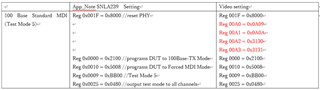
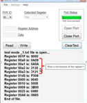
In the video titled below, data is set in registers 0xa0 to 0xa3 of the PHY.
"Reduce design time with easy IEEE 802.3 compliance with TI's industrial Gigabit PHY family DP83867"

but, the PHY datasheet does not mention addresses 0xa0 to 0xa3.

What is the function of this register?

The video can be seen from the page below the URL below.
https://www.ti.com/product/DP83867IS


See around 3:00

thank you.

Satoshi I

  • Hi Satoshi,

    Thank you for your question. Please stick to the regular configuration of DP83867 for compliance testing. Are you seeing issues with your design when conducting compliance?

    Sincerely,

    Gerome

  • Hello Gerome

    Thank you for your response.

    I'm having a problem with not passing the compliance test.
    The test is 100 Base Standard MDI (Test Mode 5) overshoot.
    As shown in the figure below, it exceeds the standard value of 5%.


    However, after setting a0 to a3, the overshoot disappeared.


    Check the registers at addresses a0 to a3.
    I understand the following, but is it correct?

    ・Information about this register is private.

    · The user never needs to use this register.

    · During the compliance test, the test will pass even if this register is not manipulated.
    (Refer to "App_Note SNLA239 Setting" for registers operated during testing)


    ・The reason for not passing the test is outside the PHY.
    (Board design, transformer/RJ-45 compatibility, etc.)

    Satoshi I

    Regards,

  • Hi Satoshi,

    I will need to get back to you regarding this. However, can you see what happens if you keep the reg 0xA0, 0xA1 settings default while keeping 0xA2, 0xA3 programmed? I would like to see which settings have the highest effect on compliance. 

    Sincerely,

    Gerome

  • Hi Gerome

    I set data only for 0xA2 and 0xA3.
    As a result, the overshoot disappeared.


    for your reference, the values of a0 to a3 are listed

    0x00a0 data:0x0907
    0x00a1 data:0x0608
    0x00a2 data:0x3130
    0x00a3 data:0x3131


    Satoshi I

    Regards,

  • Hi Satoshi,

    Thank you for the data. Please allow me to consult with my team. I expect a response by tomorrow.

    Sincerely,

    Gerome

  • Hi Satoshi,

    I apologize for the delay in my response. After talking with our team, this field (0xA2, 0xA3) is a line driver filter programming.

    Sincerely,

    Gerome

  • Hi Gerome

    Thank you for your kind cooperation.

    I have some questions about 0xA2 to 0xA3.

    ・As you said, this register seems to be a line driver filter.
    (When the value was changed, the amplitude and overshoot of the signal changed)
    In order to deepen my understanding, could you please send me a register map that describes the function of this register?

    ・I think that this register is very useful at the time of compliance test.
      Why isn't it listed in the data sheet?

    ・If the register value is changed to the value below, the compliance test will pass.
    Is it okay to change the register value during normal use?
      0x00a2 data: 0x3130
      0x00a3 data: 0x3131

    Satoshi I

    Regards,

  • Hi Satoshi,

    This register is for line drive filtering. Altering this bit field will adjust rise and fall times. We do have passing results with default values for 0xA2/3, but these values are very application specific.

    We will look to update the datasheet.

    Sincerely,

    Gerome