This thread has been locked.

If you have a related question, please click the "Ask a related question" button in the top right corner. The newly created question will be automatically linked to this question.

TCA5405: Internal structure of TCA5405, PD for DIN

Part Number: TCA5405
Other Parts Discussed in Thread: LSF0101, 2N7001T, TXU0101, SN74LVC1G07

Hello E2E Experts,

Good day.

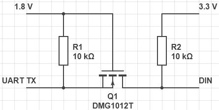
Please share the internal structure of the TCA5405 to understand what should be the value of the pull-down resistor in the attached push-pull level conversion logic. The datasheet is very stingy with details.

translated-push-pull.zip

Thank you in advance.

Regards,

CSC

  • The datasheet specifies the maximum leakage current as 0.1 µA. So the keep the voltage drop less than 1 V, the resistance must be less than 10 MΩ.

    Just use 10 kΩ.

  • CSC,

    To further explain Clemens answer

    VCC = 3.3V

    VIL (max) = 0.3 * VCC = 0.3 * 3.3V = 0.99V

    In order to pull DIN below the maximum voltage input for a logic low (VIL), you need a resistance < VIL (max) / I(i) = 0.99V / 0.1uA = 9.9Mohm.

    Choose a resistor that is less than 9.9Mohm and also satisfies min and max switching frequencies for DIN (1MHz to 10kHz). Larger resistance = greater RC = longer fall-time. If the fall-time is too long, the voltage on DIN might now have enough time to fall below a logic LOW before switching again. 

    For simplicity sake, 10kohm will work just fine as Clemens has suggested. Just thought I would add a bit of explanation on how he got there.

    Regards,

    Tyler

  • Hello Tyler,

    Good day.

    Part of the question was whether this logic would work at all, and that cannot be judged by knowing only the current. Ticket CS1218413 I linked says "You'll likely see more current draw with an external 10k." You are now offering these 10k. Also, that ticket said "first falling edge on DIN being used to turn on the internal oscillator", which is not a very clear statement in the context of the designed push-pull level conversion. For example, when the MCU is not transmitting, the level will be low. Does this mean the IC ports will go to the default state?

    So I want a clear answer about the correct IC power sequence and whether 10k to GND is the right solution that won't cause unwanted switching of the outputs (e.g. when the MCU is not transmitting) or leakages.

    Regards,

    CSC

  • The DIN input of the TCA5405 must never float. So with this two-transistor level converter, you always need a pull-down resistor.

    The TCA5405 activates when it detects a high-to-low edge at its input. (So the idle state should be high.) If the 1.8 V powers up later than the 3.3 V, then the DIN input will be initially low. I do not know if the TCA5405 detects an edge if the input is low at startup.

    You can replace this circuit with an integrated level translator like the 2N7001T, TXU0101, or LSF0101, but it is also possible to build a non-inverting translator with a single N-channel MOSFET:

    (This circuit has no dependency on power sequencing, and outputs high when the MCU is disabled. Use any MOSFET that works at 1.8 V.)

    You can also replace Q1 with an open-drain buffer like the SN74LVC1G07.

  • CSC,

    Ticket CS1218413 I linked

    I do not see this ticket in the thread, or in the ZIP file provided. Could you relink in the next response? I think there may be some information here that I am missing to help with your question. 

    Please let me know if Clemens' answer helps in any way.

    Regards,

    Tyler

  • Hello Tyler,

    Good day.

    You may disregard the ticket number.

    Below are additional information from the customer:

    The reason of using push-pull is because the IC is not good at all on EMI/EMC. Pull-up is worst than pulling by voltage directly.

    1.8v created from 3.3v, so yes, it comes later.

    Output high when MCU is disabled (Hi-z) with our circuit as well, isn't it?

    Please clarify what problem do you see with the power sequence wtih push-pull translation logic. It's not very clear from your response.

    Sorry, I'm not sure what I meant when wrote "output high".

    Yes, DIN will be low when MCU is disabled (Hi-Z on output1_mcu) with this push-pull translation logic because of the PD on DIN. Do you say this is a problem? What exactly? Will it lead to Q0-Q4 ports reset?

    One of the option then is to place PU from 1.8v to output1_mcu then, to keep gate energized and VTT2A opened when MCU is disabled

    Regards,

    CSC

  • CSC,

    The reason of using push-pull is because the IC is not good at all on EMI/EMC. Pull-up is worst than pulling by voltage directly.

    What frequency is the customer operating the IC at? I am interested because the max recommended operating frequency is < 1MHz. I am surprised that customer system is being effected by EMI/EMC effects at such frequency. 

    1.8v created from 3.3v, so yes, it comes later.

    I understand that in your current circuit, that 1.8V supply comes later because it is converted from the 3.3V supply. 


    Output high when MCU is disabled (Hi-z) with our circuit as well, isn't it?

    Please clarify what problem do you see with the power sequence wtih push-pull translation logic. It's not very clear from your response.

    Sorry, I'm not sure what I meant when wrote "output high".

    I am confused at parts in this explanation, but I will give my best response. 

    If your system is powering at 3.3V and the 1.8V supply comes later, it seems that there will be a time period where DIN will be floating. If 1.8V is close to 0V, then the bottom FET will be HIGH-Z, this means that the gate voltage of the top nFET is at 3.3V, which means that the top FET is off. This means that DIN is floating, unless there is a pull-up/down resistor available to bias the voltage at DIN. 

    It is best to never leave DIN pin floating. Also do not apply voltage to DIN when VCC is not fully powered up. 

    Yes, DIN will be low when MCU is disabled (Hi-Z on output1_mcu) with this push-pull translation logic because of the PD on DIN. Do you say this is a problem? What exactly? Will it lead to Q0-Q4 ports reset?

    Purpose of the PD on DIN is to keep DIN in a known state (logic LOW) upon startup of the device. It is best practice to keep DIN from floating. I don't think the PD is a problem. 

    Resetting Q0-Q4 occurs when a POR (power-on-reset) condition is met. This voltage level is around 1V. If you need the device to reset, power down to GND before powering back to VCC for successful reset. 


    One of the option then is to place PU from 1.8v to output1_mcu then, to keep gate energized and VTT2A opened when MCU is disabled

    I am not seeing how adding a PU from 1.8V to output1_mcu will effect the outcome of the circuit differently since 1.8V comes later from powering of 3.3V supply. I think a pull-down resistor at DIN will still be required for proper functionality. 

    Regards,

    Tyler

  • Hello Tyler,

    Good day.

    >>What frequency are you operating the IC at? We are interested because the max recommended operating frequency is < 1MHz. We are surprised that your system is being affected by EMI/EMC effects at such frequency.

    It's not about our system, it's about your EVB. All problems we had when we evaluated your IC on your EVB. It can switch from "a magic of hand" - you move a hand in 10cm from the PCB and it triggers ports. It's expectable for the IC that has proprietary 1-wire protocol which has zero protection (unlike I2C)

    >>It is best to never leave the DIN pin floating. Also do not apply voltage to DIN when VCC is not fully powered up.

    This means that the only solution for ANY design is PD on that pin! Always! Because it is a loop: how do you suppose to have PU on DIN to keep it not floating during powering up VCC and at the same time have zero on that pin when VCC is not presented? What kind of power sequence can meet this logic? None. So PD is the only solution for any design then. Logical?

    >>We are not seeing how adding a PU from 1.8V to output1_mcu will affect the outcome of the circuit

    It depends on this:

    >>I don't think the PD is a problem.

    If you believe that DIN to GND will not reset Q0-Q4 statuses then yes, this PU from 1.8V is not needed.

    I look forward to your response.

    Regards,

    CSC

    .

  • TI-CSC,

    It's not about our system, it's about your EVB. All problems we had when we evaluated your IC on your EVB. It can switch from "a magic of hand" - you move a hand in 10cm from the PCB and it triggers ports. It's expectable for the IC that has proprietary 1-wire protocol which has zero protection (unlike I2C)

    I assume then device is being used within frequency spec. I know from past use of this device, it can potentially run into issues with environments that have high EMI exposure, triggering unwanted LOWs on DIN causing error in the output. 

    This means that the only solution for ANY design is PD on that pin! Always! Because it is a loop: how do you suppose to have PU on DIN to keep it not floating during powering up VCC and at the same time have zero on that pin when VCC is not presented? What kind of power sequence can meet this logic? None. So PD is the only solution for any design then. Logical?

    My apologies.

    To come back to your original question, are you still trying to determine what the pull-down resistor value should be in the attached push-pull level conversion logic, or are there other questions of concern that you need answered?

    Regards,

    Tyler