Other Parts Discussed in Thread: USB2ANY
Hi Nicholaus,
would you please help review the updated schematic and layout?
design material
https://txn.box.com/s/l2k78zg4w4pn9wvdmv7kh3yxspsgo0
Thanks for your help!
previously E2E post
BR,
Scott
This thread has been locked.
If you have a related question, please click the "Ask a related question" button in the top right corner. The newly created question will be automatically linked to this question.
Hi Nicholaus,
would you please help review the updated schematic and layout?
design material
https://txn.box.com/s/l2k78zg4w4pn9wvdmv7kh3yxspsgo0
Thanks for your help!
previously E2E post
BR,
Scott
Hi Scott,
Thank you. Please allow some time for the review, and I will get back to you ASAP.
Regards,
Nicholaus
Hi Scott,
I've been having an issue opening these files. Can you open them?

Regards,
Nicholaus
Hi Scott,
As I have said in the e-mail, it is important that the files are uploaded here so that we can refer to them in the future. Could you try posting them again?
I have received the schematic and layout files and will review today.
Regards,
Nicholaus
Hi Scott,
It looks like the customer only followed my advice on the power supply, but did not make the other recommended changes. I will follow-up with the layout review.
High Speed Differential I/Os
PET: 0.22uF coupling caps on the TX side
PER: Ok, no caps on RX side.
Reference Clock
REFCLK: Connected to PI6CB33201 PCIe clock buffer
REFCLK_OUT: Floating
JTAG
TDI: Floating
TDO: Floating
TMS: Floating
TCK: Floating
TRST#: *Floating, recommend 1K to GND if not using. System noise could cause unintended failure.
Control
ICC_1: Floating
ICC_2: Floating
ICC_3: Floating
RX_DET_BYP: 20K to GND, auto RX detect
WIDTH: Floating, 1x8 link-width.
PCI-Express Auxiliary Signals
CLKREQ#: *100K pullup to 1.8V. CLKREQ# is deasserted by default. Assuming EGPU will pull this low to avoid L1.1 state.
PERST#: Being controlled by EGPU.
PRT1_RST#: *Floating, recommend populating R0417 pullup to 1.8V.
PRT0_RST#: *Floating, recommend populating R0415 pullup to 1.8V.
System Management Bus
MODE: Floating, link-width manager; EEPROM > 16kbit
SMBCLK: *No connection shown. Make sure there is a 4.7K pullup to 3.3V.
SMBDAT: *No connection shown. Make sure there is a 4.7K pullup to 3.3V.
SMB_ADDR_0: 1K to GND
SMB_ADDR_1: 1K to GND
* SMB_ADDR = 0x20, EEPROM Reader and Link-width Manager
EE_CLK: Has 2K pullup resistors to 1.8V, connected to 16K EEPROM
EE_DAT: Has 2K pullup resistors to 1.8V, connected to 16K EEPROM
Power
OK, separated the digital and analog supplies using ferrite bead as shown in the EVM Schematic. Must ensure 1.17V rail is always within 2% of 1.17V.
Regards,
Nicholaus
There was an Asus e-mail that I was looped into. Adding the comments here for future reference:
TRST#: *Floating, recommend 1K to GND if not using. System noise could cause unintended failure.
[Tim] We will populate R0422.
CLKREQ#: *100K pullup to 1.8V. CLKREQ# is deasserted by default. Assuming EGPU will pull this low to avoid L1.1 state.
[Tim] Yes. EGPU will pull this low to exit L1.1 state.
PRT1_RST#: *Floating, recommend populating R0417 pullup to 1.8V.
PRT0_RST#: *Floating, recommend populating R0415 pullup to 1.8V.
[Tim] OK. We will populate R0417, R0415.
SMBCLK: *No connection shown. Make sure there is a 4.7K pullup to 3.3V.
SMBDAT: *No connection shown. Make sure there is a 4.7K pullup to 3.3V.
[Tim] It’s in page 5. Sorry, forgot to put this page into schematic.
Hi Nicholaus,
Thanks. would you please provide feedback on layout?
BR,
Scott
Hi Scott,
I am running simulations to see if I can offer any more design-specific examples, but for now the customer can continue to add the layout updates I requested earlier. It looks like they have fixed the Intra-Pair Skew issue, but did not address the other issues I mentioned. I also added the new recommendation to add void under the Tx capacitors as described in High-Speed Guidelines for Signal Conditioners.
Vias:
Backdrilling: Please ensure that all high-speed vias between Top-In1 or Bottom-In3 are back-drilled so that stubs are not created as described in Section 4.6 of the High-Speed Guidelines for Signal Conditioners document
Ground Vias: Add ground vias near high-speed signal vias to ensure consistent ground and minimal impedance change as described in Figure 10 of High-Speed Guidelines for Signal Conditioners
Traces:
Intra-Pair Skew: OK, all traces are <5 mils difference for all PCIe high-speed channels.
Void Under Capacitors: add GND void under capacitors
Regards,
Nicholaus
Hi Scott,
One other question. Is the 100MHz clock that goes to the retimer also routed to the PCIe endpiont and the CPU?
The retimer only supports a clocking topology where the retimer and the CPU share the same 100MHz reference clock.
Regards,
Nicholaus
Hi Nicholaus,
this is still in internal forum, customer cannot access your feedback.
Would you please move this to external forum?
thanks for help!
BR,
Scott
Hi SHH,
Sorry, I thought you had the ability to do this. I tried, but I don't see the Interface forum as an option to move this issue to. I am following up with IT now.
Regards,
Nicholaus
Hi Scott,
I have oved this issue to the public forum.
Regards,
Nicholaus
Hi Nicholaus,
The 100MHz clock topology is shown in the attachment. It comes from CPU and goes to retimer and endpoint(GPU) through a clock buffer.
Hi Wen-hsin wang,
Ok that is good, the retimer supports this kind of clocking topology with no issue. Please refer to our high-speed design guide and make the following changes when convenient.
Vias:
Backdrilling: Please ensure that all high-speed vias between Top-In1 or Bottom-In3 are back-drilled so that stubs are not created as described in Section 4.6 of the High-Speed Guidelines for Signal Conditioners document
Ground Vias: Add ground vias near high-speed signal vias to ensure consistent ground and minimal impedance change as described in Figure 10 of High-Speed Guidelines for Signal Conditioners
Traces:
Intra-Pair Skew: OK, all traces are <5 mils difference for all PCIe high-speed channels.
Void Under Capacitors: add GND void under capacitors
Regards,
Nicholaus
Hi Nicholaus_Malone,
Two questions.
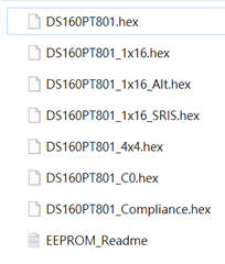
1. I got a EEPROM image from Scott. Is this a EEPROM pre-loaded image before SMT ? Which means I can use this image(hex file) to program EEPROM through a EEPROM programming socket before SMT ?
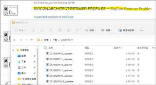
2. It seems that I need to configure DS160PT801 through SigCon Architect. But I don’t find any DS160PT801 profile or updater. Where can I get the DS160PT801 updater ?
Thanks.
Hi Wen-Hsin Wang,
The DS160PT801 SigCon Architect profile and SigCon Architect framework is not in SIGCONARCHITECT-RETIMER-PROFILES. It is available in a different MySecure folder. Please send me your e-mail through direct message and I will grant access.
Regards,
Nicholaus
Hi Nicholaus,
I send you Wen-Hsin and my email. please grant access to us. thanks.
BR,
SHH
Hello,
Access should be granted. Let me know if there are any issues.
Regards,
Nicholaus
Hi Nicholaus_Malone,
I have a question.
I am confused about the role of retimer master and slave mode.
Can DS160PT801 be accessed by host(system controller such as EC or PCH) through SMBUS when DS160PT801 is configured as EEPROM reader(Master)?
Hi Nicholaus,
add one more question,
1.I am confused about the role of retimer master and slave mode.
Can DS160PT801 be accessed by host(system controller such as EC or PCH) through SMBUS when DS160PT801 is configured as EEPROM reader(Master)?
2. can customer use third party EEPROM programming to program the hex file before SMT?
BR,
SHH
Hi Scott,
1. Yes, the retimer can communicate through SMBus independent of it's role as EEPROM reader or listener.
2. Yes, they can.
Regards,
Nicholaus
Hi Nicholaus,
1. The PCB is back but it can't work. We have checked power, CLKREQ# and PERST#. All of these signal seems good. Do you have any recommendation for further debug ? Which retimer's register can we read to check retimer's condition ?
2. The EEPROM FW I use is DS160PT801.hex. Is that OK for my topology ?

Hi Scott,
1. Did they make the changes I recommended to the board they built? If so, would you mind taking a screenshot of the high-level page of SigCon Architect so we can see the retimer status? What does "can't work" mean? Does the system not achieve a PCIe Gen1 link?
2. This EEPROM should be OK. The link width for this application is 1x8 correct?
Thanks,
Nicholaus
Hi Nicholaus,
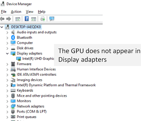
1. "Can't work" means the GPU does not appear in device manager when system power up.
2. We will try to modify PCIE speed configuration from BIOS to see if system can achieve PCIE GEN1 or not.
2. Yes. 1x8.
Hi Scott,
If the customer didn't follow the recommended layout changes and they are unable to achieve Gen3/Gen4, it could be a signal integrity issue. However, the GPU should automatically drop to PCIe Gen1 and see the device in the Device Manager. I don't expect the BIOS change to make a significant difference.
Please take a screenshot of the high-level page of SigCon Architect to start.
How long is the cable in this application? If you use a short cable, do the results change?
Thanks,
Nicholaus
Hi Scott,
To answer your e-mail question. The DPS dongle eventually turned into the USB2ANY, which is available here: USB2ANY Evaluation board | TI.com
Second question regarding how to use SigCon Architect. Please refer to the DS160PT80X16EVM for instructions on how to use SigCon Architect.
DS160PT801X16EVM Evaluation board | TI.com
If the customer wants to use SigCon Architect with their own custom board, they will need to get a USB2ANY as mentioned above, and connect it to their SCL/SDA I2C lines. After that, the process will be the same as the EVM. Let me know if you need help with this.
Regards,
Nicholaus
Hi Tim,
I send you the USB2ANY EVM. please let us know if any questions.
BR,
Scott
Hi Nicholaus,
1. The high level page screenshot. Looks like some channel loss signal ?
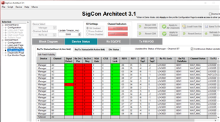
2. The cable length is approximately 16 inch.
Hi Wen-Hsin Wang,
If channel loss was an issue, I would expect this to fail at PCIe Gen4 or Gen3 speeds, but it should downgrade to a Gen1 link.
The high-level page shows that Channel B2 is not detecting a signal. I recommend investigating channel B2 and ensure the signal is successfully reaching the DS160PT801.
Regards,
Nicholaus
Hi Nicholaus,
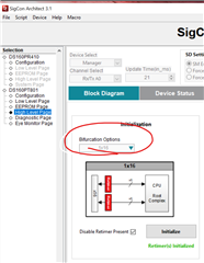
We adjust the "Bifurcation options" from 1x16 to 1x8 and the system reach the DS160PT801 successfully. The Nvidia graphic driver also appears in device manager. But I have no idea why the Bifurcation options shows that the system is 1x16.
Hi Nicholaus,
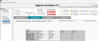
We adjust the "Bifurcation options" from 1x16 to 1x8 and click Initialize button. After restarting the system, it reach the DS160PT801 successfully. The Nvidia graphic driver also appears in device manager.
But I have no idea why the Bifurcation options shows that the system is 1x16. Are there any registers we can read from the Low Level Page or EEPROM Page to see if the link-width setting is correct or not ?

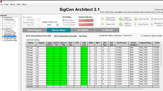
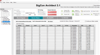
Besides, I capture some images from the system which can successfully achieve PCIE GEN4 link. We have some questions.
1. What does VGA Gain mean? Is VGA Gain the same as pre-emphasis ?
2. According to the images, are the PCIE signals good ? Do we need to modify any settings to improve PCIE signal quality ?
Thanks.
Hi Wen-Hsin Wang,
After the system is restarted it is likely that the registers were reset and the link-width setting "1x8" was changed back to "1x16". If the link was successfully established, it suggests there is no issue. I'm unsure why it started working when you performed this change.
Yes, you may look at the Configuration Guide on MySecure for the register map. It will show you that 0xF2 and 0xF3 are the link-width registers.
1. VGA Gain is a variable gain amplifier that is present at the Rx of the retimer, it is automatically adapted to the best setting and shouldn't be changed. It is not the same as pre-emphases, which is a Tx signal conditioning technique.
2. It looks good, but it would be better to perform PCIe system testing to ensure the signal quality is good. The retimer can only show what the signal quality lookes like in the retimer, not what it looks like on the far-end near the root complex or endpoint. The retimer automatically adapts all of its signal conditioning settings to the best value, so its settings do not need to be modified like a redriver.
One more thing, it looks like they are using SigCon Architect 3.1. The version in the MySecure folder is SigCon Architect 3.2. I recommend the customer update to the latest version.
Regards,
Nicholaus
Hi Nicholaus,
1. I capture the images about 0xF2 and 0xF3 register data while system power up. Looks like it is a x16 link-width. But it's weird. The EEPROM_Readme file says that the link-width is determined by the 'WIDTH' pin setting and our 'WIDTH' pin is floating, so it's supposed to be a x8 link-width. Not sure why it becomes a x16 link.
How does retimer determine the link-width ? Does the link-width not only determined by the WIDTH pin ?
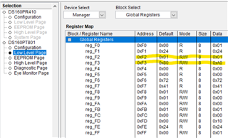
2. Can we modify the EEPROM data to force the link-width to 1x8 through Sigcon Architect?
1. You are correct, if you use the DS160PT801.hex file, which does not load a link-width setting into the 0xF2 or 0xF3 registers, the link-width setting should be whatever the pin-strap setting is. According to the datasheet, a floating link-width pin is not 1x8. It is the register default setting, which is 1x16. Do you have the latest datasheet?
If the width pin is floating, the link-width setting is determined in order by:
1. The default register setting in 0xF2 and 0xF3, which should be 1x16.
2. The current register setting, whether it is loaded by EEPROM or manually changed through I2C.
There are two ways you can force the link-width to 1x8 when the link-width pin is floating:
1. Set the 0xF2 and 0xF3 registers to 1x8 in the EEPROM image.
2. Write to the 0xF2 and 0xF3 register a link-width of 1x8 before PCIe link training begins.
You can also force the link-width to 1x8 by changing the pin-strap setting to level-3 (10K to PWR_1)
Regards,
Nicholaus
The datasheet I got is too old.
The system is normal after I change the pin-strap setting to level-3.
Thanks ~
Hi Nicholaus,
Another issue.
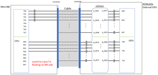
So far the x8 model is normal. But it is abnormal when using the same external GPU device connect to a x4 notebook. The symptom is the same as before. The GPU does not appear in the device manager.
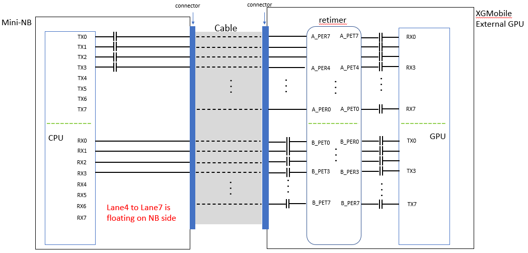
The topology is shown below.
My question is:
1. Does retimer support 1x4 ? According to the datasheet, I only can see it support 2x4.
2. I have tried to modify the "Bifurcation Option" to 1x4 and 2x4 from Sigcon Architect but still can't fix this issue.
3. I have tried to modify the strap pin setting to level-1 but still can't fix this issue.
4. According to the topology. Which link-width setting should I set ? 1x4 or 2x4 ?
Hi Wen-Hsin Wang,
Best,
David
Hi David,
The external GPU appears in device manager while in x8 mode with x4 notebook. Looks like the problem is solved by changing retimer to 1x8 mode.
But the GEN speed is only PCIE GEN1. Not sure what's going on because the GEN speed can reach to PCIE GEN3 in x8 mode with x8 notebook.
I capture some images from Sigcon Architect. Can you please help to check ?
Thanls.
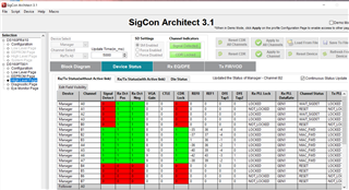
Hi Wen-Hsin Wang,
It appears that channel B0 does not see a signal in this configuration, but from your block diagram it should be routed from GPU to the retimer. Please ensure that this channel is connected appropriately.
Best,
David
Hi David,
1. I try another x4 notebook. Each channel looks good but the GEN speed is still GEN1.
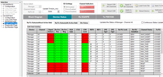
2. Is this issue related to channel length ? The PCIE length of the x4 notebook is very short, approximately 1.2 inch.
3. Since the PCIe link is successfully established, does it suggest that the retimer is OK ? Maybe the GEN speed problem is caused by host ? Maybe I should try to change the preset value ?
Hi Wen-Hsin Wang,
I don't believe that this is an issue with channel length. It appears that the retimer can detect all signals and is locking at Gen1. Is the host capable of Gen4?
Best,
David
Hi Wen-Hsin,
Got it, thanks. Let me investigate a bit further and get back to you.
Best,
David
Hi Tim, Scott,
Please keep me updated on this issue based on what we discussed in-office.
Best,
David
Hi David,
I have reported the routing issue to my director and I am still working on how to modify it.
Besides, there is another question. Even though the routing is wrong, the link is still established successfully but it is in "compliance mode".
Why does the link can enter the "compliance mode" if I set the "Bifurcation options" to 1x8 but fail if I set to 1x4 ?
Hi Wen-Hsin,
I believe the link is able to enter Gen1 compliance mode due to the detected RX terminations on four lanes A/B4-7. If I remember correctly (based on this image below), all channels A4-A7 and B4-B7 are terminated, while channels A0-A3 are unterminated. To my knowledge in x4 mode, the retimer is looking for termination and signal on lanes 0-3, not lanes 4-7. So, in x8 mode, the retimer detects 4 lanes of active traffic on lanes 4-7 and begins transmitting a compliance pattern on those lanes, while leaving lanes 0-3 idle.
