This thread has been locked.

If you have a related question, please click the "Ask a related question" button in the top right corner. The newly created question will be automatically linked to this question.

DS90CP04: DS90CP04 CLK Link Risk assessment

Part Number: DS90CP04

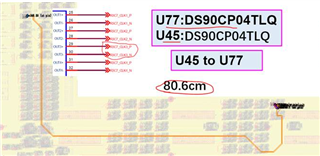
Many TI DS90CP04 clock drivers are used in our project, and the longest topology is as follows: U77 transmitter and U45 receiver both use DS90CP04 chip:

The longest CLK length is 80.6cm, and the maximum clock frequency that needs to be supported is 700MHz For such link topology, we have the following problems and need your strong support. Thank you
1.What is the maximum link length supported by DS90CP04 chip at 700MHz clock frequency? Is there any test data from TI?(Our design link is too long. How do we identify our design risk?)

2.What methods do we have to evaluate the reliability of DS90CP04 chip link topology?

3.n the IBIS model of DS90CP04 chip on TI's official website, the reflection after connecting the driver end is particularly large during the simulation. What should we pay attention to when using DS90CP04 chip to run CLK SI simulation to evaluate the link length? (Simulation frequency 700MHz)

4.Is the input/output of DS90CP04 internally physically switched or redriven?


  • Hi Zeliang,

    1). DS90CP04 is a cross point/buffer. Device is characterized to deliver AC performance shown in electrical characteristics(LVDS output). IOutput performance was not characterized over a certain transmission media.

    2). Please note LVDS output and switching characteristics noted in the data sheet. Using s-parameter of your transmission media, you can do analyses to determine performance and reliability.

    3). Using your transmission media with the end point s-parameter could be used to optimized return loss(i.e reduce reflections).

    4). I believe it is both: first it is buffered, then switched before the output drivers.

    Regards,Nasser

  • Ok, thanks for the professional guidance