A related question is a question created from another question. When the related question is created, it will be automatically linked to the original question.
If you have a related question, please click the "Ask a related question" button in the top right corner. The newly created question will be automatically linked to this question.
In the TX mode the A/B pins can be left floating as they are outputs - but the input should be pulled to known logic level so that the TX pins are oscillating and possibly radiating energy from the open pins.
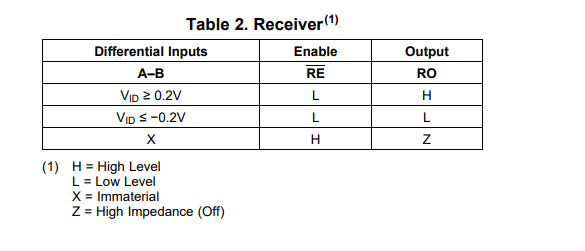
In the RX mode of the device the A/B pins should not be left open/floating if unused. The voltage between A and B needs to be >= 200mV or <= -200mV or else the output pin can glitch since the logic level is indeterminate on the A/B pins. If unused A or B need to pulled high and the B or A need to be pulled low so that the differential voltage is at a known valid logic level. to prevent glitching at the output (RO) pin. So for RO to have a logic one output A is HIGH and B is LOW, and if RO is going to have a output of ~GND then A should be pulled LOW and B should be pulled HIGH.
If you have any other questions please let me know and I will see what I can do!
For differential bus inputs please see table 2 (pg 2) - driver doesn't matter as an unused output can remain floating without much concern. but since this is half duplex A and B can be a receiver also
VID ratings are only defined above 200mV and below -200mV - in-between those thresholds the input is in an indeterminate logic state (which is implied, but not explicitly stated) - which means the "R" pin can be high or low - or switch between the two randomly. If there is termination on the bus the calculations to set the idle voltage on the bus is detailed in this application note: https://www.ti.com/lit/an/slyt324/slyt324.pdf
If there is no termination - pulling A to VCC and B to GND will set the VAB voltage to ~VCC which while the device is active will register as a logic 1 at teh "R" pin and you have a known logic. Since "R" is an output and isn't glitching it can be left floating if unused.
For DE, /RE and D input pins its not explicitly stated in the datasheet - they are implied via the VIH and VIL ratings under the driver electrical specifications (for pins DE and D on pg 4) where VIL and VIH are 0.8V max and 2.0V min respectively.
For the /RE pin the VIL and VIH are the same as driver logic pins (0.8V max for VIL and 2.0V min for VIH) and the rating is shown on pg 6.