A related question is a question created from another question. When the related question is created, it will be automatically linked to the original question.
If you have a related question, please click the "Ask a related question" button in the top right corner. The newly created question will be automatically linked to this question.
I have reviewed the schematic and it looks very good. I do have the following comments for your consideration.
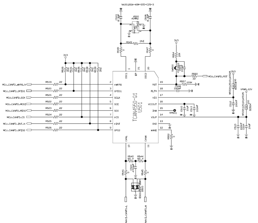
The nINT and GPO2 pins are open-drain and need a pullup resistor. The pullup resistors in the schematic are DNI, so these would need to be installed in order to use these two pins to return interrupt status to the MCU.
The SPI nCS pin should be High when the SPI bus is not active. If the MCU will drive the nCS pin High, then the DNI pullup resistor in the schematic can remain DNI. However, you may want to consider installing this pullup resistor to ensure the pin is High when SPI is not active.
The crystal oscillator components look good to start and I recognize the values are similar to the TCAN4550 EVM. However, you should still optimize this circuit to ensure it is stable on your board and across your desired operating conditions. See the TCAN455x Clock Optimization and Design Guidelines application note for more information.
The Inhibit (INH) pin does not appear to be used, which is OK, and it is only connected to a test point. This pin is is driven High when the device is active, but becomes Hi-Z when the device is not-active. Normally when used, there should be a pulldown resistance to discharge the voltage from the parasitic capacitance and hold the line Low. Without a pulldown resistor, this discharge could take a bit of time. No changes to the schematic are required, but just keep this in mind when making measurements with this test point.
By default the nWKRQ pin is driven High to 3.6V which is an internal rail derived from the VSUP supply so that it is active when the device is in Sleep Mode. So if it is left in the default configuration it does not need a pullup resistor.
However, it can be configured to be an open-drain type of pin to use a pullup resistor to the VIO rail by setting the nWKRQ_VOLTAGE bit (0x0800[19]) to "1".
Most MCU's should be tolerant of 3.6V, but this would need to be verified for the specific MCU you are using. If the MCU is not tolerant of 3.6V, then this could be divided down with a couple of resistors or switched to the open-drain configuration requiring a pullup resistor to 3.3V.