This thread has been locked.

If you have a related question, please click the "Ask a related question" button in the top right corner. The newly created question will be automatically linked to this question.

TL28L92: Data Sampling edge mismatch

Part Number: TL28L92

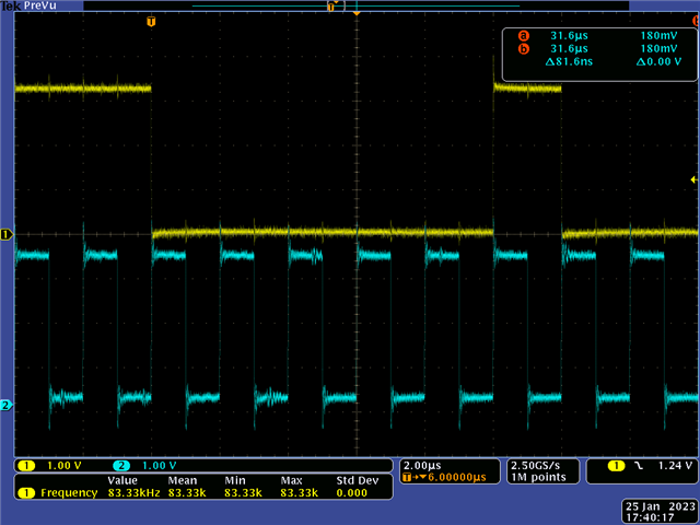
We are facing an issue while transmitting data. As per data sheet, when the external clock is used by the transmitter in pin IP3, the transmitted data is clocked on the falling edge of the clock. But our transmit data when probed on an oscilloscope shows the converse. Please see the attached scope image.
Also, we don't find a method in the datasheet to reverse the edge polarity. Why does this happen?

The DUART chip configuration is given below:

Normal mode
16 byte FIFO
interrupt when one or more bytes are received
disable watchdog
RxRTS control on
RxRDY interrupt enabled
block error mode
no parity
8 bits/char
normal channel mode
no TxRTS control
CTS enable of transmit
1 stop bit
receive clock = IP4 (1x)
transmit clock = IP3 (1x)

The DUART pin level details are attached.

  • Hi Divya,

    Just for clarity, is channel 2 in your scopeshot the IP3 pin and channel 1 the TxDA pin?

    Do you have a schematic we could review?

    -Bobby

  • Hi Bobby,

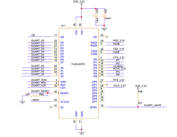
    Channel 1 is the TxDA pin and Channel 2 in the scope image is the OP2 pin which is configured as channel A transmitter 1× clock. This follows the input at IP3 pin, where a 0.5 MHz clock is connected. Please find the attached snapshot from the schematic.

    Also, for your information;

    I/M is left floating.

    Data lines, address lines, RD/WR/CE lines are connected to EBI of MCU.

    0.5 MHz to IP3 is provided by an MCU Timer. 

  • Thanks Divya,

    I'm trying to reach out to one of our digital design engineers who should be able to look at the internal logic of the device. He should be able to verify if the data is sampling on the wrong edge in the design and check to see if there is a way to flip the sampling edge. 

    -Bobby

  • Hi Bobby,

    We are under significant pressure on this wrong sampling edge issue. This issue has stopped us a major release to customer. Your response is highly appreciated. Please help.

    Regards,

    Siju Krishnan

  • Hi Siju,

    The design engineer got back to me this morning. It seems that the serial data transmission of the TxD pin is launched from the rising edge of the clock, he has verified that there is not a way to modify this to occur on the falling edge.

    -Bobby

  • Hi Bobby,

    As per datasheet, the TXD will clocked on falling edge of the clock and RXD will be sampled at rising edge.

    Does that mean datasheet is wrong?

    Regards,

    Siju

  • Hi Bobby,

    This is a complex issue for us now, we have to go back to the end customer with a definitive solution. Please provide a conclusive answer.

    1. Has TL28L92 datasheet got any error related to sampling edge or TXC and RXC ?

    2. If yes, are you going to revise the datasheet or the device?

    Based on these inputs we have to plan on the next steps. A quick response is expected.

    Regards,

    Siju

  • Hi Siju,

    Based on the scopeshots you provided and the input from our design engineer, it seems like the TxD transmission edge is incorrect in the datasheet. 

    Yes, we do plan on revising the datasheet. Currently there is a correction to the datasheet we need to make regarding the multi-drop mode to the device, after that revision we will update the transmission edge error on TxD.

    -Bobby

  • Hi Bobby,

    Thanks for the confirmation. However, the correction has to apply on RXC as well. The RXD sampling is happening on the falling edge not on rising edge as described in datasheet.

    I wonder the device is in market more than a decade now, no one faced this issue so far!

    For us, we lose a whole lot of money and time to spin a PCBA because of this issue. It's worrisome.

    Regards,

    Siju

  • Hi Siju,

    Sorry to hear about the issue you're facing. It seems like we hadn't had customers report any errors with this device until recently (my guess is when the competitor device was obsoleted). 

    I've talked with my manager and we are planning to make an internal evaluation module (EVM) for this device to try to validate all features/functionality listed in the datasheet of it the best we can. Hopefully we can remedy this better future use of this device.

    Our current timeline is approximately 2 months to get a board designed and ready then maybe 2 weeks to get hardware and code up and running to to try validate the device.

    -Bobby