


Part Number: TCA39306
TCA39305 support team
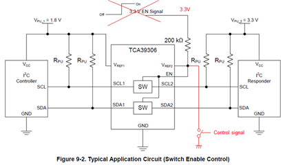
Figure 9-2 is recommended for controlling SW enable.
Is it possible to directly connect VREF2 and EN terminal to GND for SW control as shown below?
If NO, why is it?
Thanks
Tamio
Part Number: TCA39306
TCA39305 support team
Figure 9-2 is recommended for controlling SW enable.
Is it possible to directly connect VREF2 and EN terminal to GND for SW control as shown below?
If NO, why is it?
Thanks
Tamio


