A related question is a question created from another question. When the related question is created, it will be automatically linked to the original question.
If you have a related question, please click the "Ask a related question" button in the top right corner. The newly created question will be automatically linked to this question.
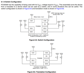
PCA9306: About Switch Configuration and Translation Configuration
In addition to Clemens' response, we generally recommend a value of ~10uF for the bypass capacitor. However, if the current capacitor you are using mitigates the noise seen, then it is ok.
Also note that external pull up resistors are needed for proper I2C communications for this device. If not readily available, both setups (Case 1 and Case 2) can be used with the TCA9406 as the device features internal 10k pull up resistors on all 4 data lines (SCL/SDA)
Edit (2/17/23)- Changed "10uF for the bypass capacitor" to say "0.1uF"
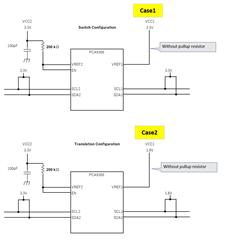
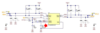
I am understanding how to use the PCA9306 step by step. I redesigned my schematics. Please see the following modified schematics. I have four questions.
(1)Is the following modified schematics OK?
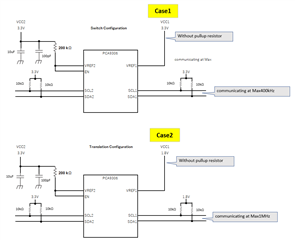
(2)Do you mean that the communicating speed is Max400kHz in Switch Configuration?
(3)Do you mean that the communicating speed is Max1MHz in Translation Configuration?
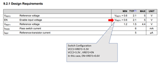
(4)In Switch Configuration(VCC1=VCC2), Is it OK that EN connect VREF2 at 3.3V( through a 200-kΩ resistor)? I concern that the 9.2.1 Design Requirements of datasheet descripts EN>VREF1+0.6V.
2/3. The maximum speed depends on the parasitic capacitances of your circuit, and cannot be predicted. Check the rising edges with an oscilloscope, and adjust the pull-up resistors accordingly.
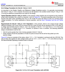
4. The PCA9306 datasheet does not mention the switch configuration. See section 9.2.4 of the LSF0102 datasheet.
I cannot understand question No.4. Because I saw section 9.2.4 of the LSF0102 datasheet but there isn't description of vrefA=vrefB(switch configuration).
I want to know clearly that PCA9306 is enabled or not on Case1 schematic (VCC1=VCC2=3.3V and EN is connected VREF2).
The switch configuration (VREF1 = VREF2 = 3.3V) will work as the device will be enabled by the EN pin shorted to VREF2. The 0.6V requirement is only intended if you choose to use this device as a level translator. See section 8.1.5 for more details on using the switch configuration:
If the above configuration (Figure 8-5) isn't feasible in your design, the set up you currently have will also work- just a slight increase in propagation delay time (which shouldn't be an issue since I2C is a rather slow protocol anyways)
The PCA9306 itself is an analog device and does not really need decoupling capacitors for its reference voltages, but there should be a small capacitor at EN (= VREF2) to keep the gate bias voltage stable. This capacitor is (dis)charged through the 200 kΩ resistor, so it should be small, i.e., 100 pF.
When switching, the current through the pull-up resistors changes, so it can make sense to have decoupling capacitors on those supplies. (The pull-up voltages are not necessarily identical with the VREF voltages.) The value and placement of these capacitors depends on your power supply, board routing, and placement of the pull-up resistors.