This thread has been locked.

If you have a related question, please click the "Ask a related question" button in the top right corner. The newly created question will be automatically linked to this question.

DS90UB940-Q1: DS90UB940+DS90UB927 application

Part Number: DS90UB940-Q1

Hello,

One customer used DS90UB940+DS90UB927 for his application, he has confirmed UB927 could display 720p 30fps normally with UB928.But now he didn't  know how to configuration UB940.

About UB940, RIN0 input, 4 data lanes CSI0 output, MODE0 and MODE1 pulled low.

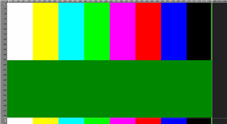
The registers of UB940 configure 0x6b=0x40,OFMT=YUV420,IFMT=RGB444. But the processor captured CSI image is 1270*360, Y direction compressed half.

If  0x6b=0x50,OFMT=YUV420,IFMT=RGB444.The processor captured CSI image is 1270*16, Y direction compress more.

MIPI CSI processor configured YUV422 format  UYVY8_2X8. 

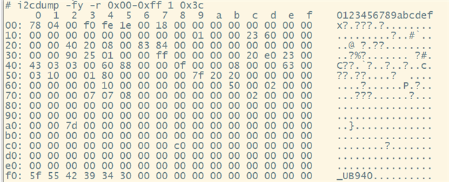
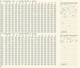
Below is UB940 and UB927 registers value. 
Best regards

kailyn

  • Hello Kailyn,

    let me review all the provided details and come back to you within the next 2 days.

  • Hello Kailyn,

    The above-mentioned registers are only for configuring the Pattern generator. Are you trying to utilize this Patgen or just output the incoming signal from the UB927?

    If you want just to output the signal coming from the UB927, then the configuration you have done with MODE_SEL0 & 1 are fine.

    One more thing you need to care about is the minimum supported PCLK with the 927 is 5MHz, while the 940 does support a min of 25MHz PCLK. 

  • Hi Hamzeh,

    Thank you very much for your reply.

    Enable UB940 pattern generator, 0x64=0x05 to generate color bars, but the phenomenon is the same with extern input signal to UB927.

    If 0x1B=0x7D,but it reads 0xB0, calculated PCLK=35.2Mhz.

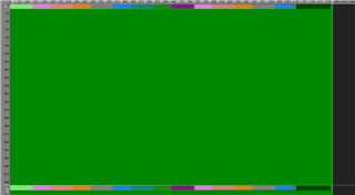
     Below is the capture image with UB940 OFMT=0100 YUV420  and OFMT=0101 YUV422_8.

    Best regards

    Kailyn

  • Hello Kailyn,

    It looks like you are using wrong timings not matching your display. Please double check the supported resolution and PCLK in your Display's datasheet.

    Also, please refer to this Appnote for utilizing our Patgen.

  • Hello Hamzeh,

    The RxCLKIN frequency of DS90Ub927 is 30Mhz. The CSI0 CLK of DS90UB940 is 105MHz

    In addition,  MIPI CSI  signal of processor is by MUX 2:1 to select.  When it is selected UB954, the image captured is no problem. But MIPI CSI selected 927, it displays is abnormal. 

    The registers configuration of UB954 are as following
    0x6d=0x7f
    0x70=0x1e
    0x7c=0xc1

    Best regards

    kailyn

  • Hello Kailyn,

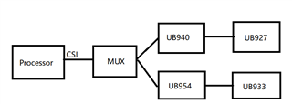
    can you please plot a block diagram showing how are these devices, i.e. 927, 940 and 954 are related to each other? 

  • Hello Hamzeh,

     Below is the block diagram.  The DS90UB954 could capture image successfully , while DS90UB940+DS90UB927 appears the above problem. Please help.

    Thank you very much.

    Best regards

    kailyn

  • Hello Kailyn,

    Thanks for providing the block diagram. It is very helpful!

    Are you sure your processor is receiving the same data from the 954 and from the 940?

    What is the data type and resolution coming from the 954?

    Can you also provide a register dump from the 940 CSI-2 indirect registers (0x00 to 0x2F)? You can dump these by writing the indirect register's address into main page register 0x6C, and then read main page register 0x6D.

    If 0x1B=0x7D,but it reads 0xB0, calculated PCLK=35.2Mhz.

    Additionally, are you expecting the value 0x7D in reg 0x1B? because this means 135MHz which is not supported by the 927!

    Enable UB940 pattern generator, 0x64=0x05 to generate color bars, but the phenomenon is the same with extern input signal to UB927.

    Are you using external CLK and timing for the patgen? If yes, can you repeat by using Internal CLK and timing from the 940.?!

  • Hello Hamzeh,

    Thank you very  much for  your reply.

    Are you sure your processor is receiving the same data from the 954 and from the 940?

    They are not receiving the same data, the input of  933 is camera, the input of 927 is another processor.

    What is the data type and resolution coming from the 954?

    1280*720

    Can you also provide a register dump from the 940 CSI-2 indirect registers (0x00 to 0x2F)? You can dump these by writing the indirect register's address into main page register 0x6C, and then read main page register 0x6D.

    UB940 CSI-2 Indirect Registers:
    Reg0x00=0x01
    Reg0x01=0x08
    Reg0x02=0x03
    Reg0x03=0x0A
    Reg0x04=0x02
    Reg0x05=0x05
    Reg0x06=0x02
    Reg0x07=0x04
    Reg0x08=0x02
    Reg0x09=0x00
    Reg0x13=0x3f
    Reg0x14=0x00
    Reg0x16=0x13
    Reg0x2e=0x00

    Additionally, are you expecting the value 0x7D in reg 0x1B? because this means 135MHz which is not supported by the 927!

    The customer refers to the description of 0X1B to configure 0X7D, and read it 0XB0, by this he could calculate the PCLK frequency.

    Are you using external CLK and timing for the patgen? If yes, can you repeat by using Internal CLK and timing from the 940.?!

    He used the internal clock and it could output correct image.

    Pattern Generator Indirect register:
    Reg0x03=0x06;
    Reg0x07=0x00;
    Reg0x08=0x05;
    Reg0x09=0x2d;
    Reg0x04=0x50;
    Reg0x05=0x05;
    Reg0x06=0x32;
    Reg0x0c=0x20;
    Reg0x0d=0x20;
    Reg0x0a=0x20;
    Reg0x0b=0x20;
    Reg0x0e=0x03;

    Main register:
    Reg0x6b=0x50;
    Reg0x65=0x04;
    Reg0x64=0x05;

    and we could find that it is correct color bars.

    Best regards

    Kailyn

  • Hello Kailyn,

    UB940 CSI-2 Indirect Registers:
    Reg0x00=0x01
    Reg0x01=0x08
    Reg0x02=0x03
    Reg0x03=0x0A
    Reg0x04=0x02
    Reg0x05=0x05
    Reg0x06=0x02
    Reg0x07=0x04
    Reg0x08=0x02
    Reg0x09=0x00
    Reg0x13=0x3f
    Reg0x14=0x00
    Reg0x16=0x13
    Reg0x2e=0x00

    I need the values of registers 0x0E to 0x12.

    He used the internal clock and it could output correct image.

    That means the customer is using wrong Patgen or bad external clk for generating the patgen.

    Please ask them do double check the 927 output. Also, make sure your 940 is using single FPD-Link mode for using that 30MHz pclk.

  • HI Hamzeh,

    Thank you for your reply. 

    UB940 CSI-2 Indirect Registers:
    Reg0x0e=0x00
    Reg0x0f=0x85
    Reg0x10=0xff
    Reg0x11=0xed
    Reg0x12=0x0e

    In addition, using UB927 pattern generator, if the 0x65=0x04 or 0x05,- the output color bar is correct. But if 0x65=0x00,the captured image is 

    1280*20.

    Best regards

    kailyn

  • Hello Kailyn,

    I have calculated your received data from the provided registers, it looks like the 940N is receiving the resolution 1280 x 665. Are these readings during Internal pattern generation or during external pattern generation?

  • Hello Hamzeh,

    Thank  you very much for your reply.

    The value of 0x0e-0x12 registers  is  read when during normal operation instead of pattern generation. 

    Best regards

    kailyn

  • Based on those readings, are you receiving the correct resolution, during normal operation?

  • Hello,

    In the pattern configuration mentioned above, if the total horizontal line width is changed from 1360 to 1350, the image cannot be captured correctly; so adjust the timing of the actual image, HBP = 32,HT = 1360, Hspw=32, VBP = 32, VT = 800,VSPW=32, images can be captured correctly, why?

    Another question that you would like to ask is that the if MODE_SEL0 and MODE_ SEL1 pulled down  and it could  capture images.

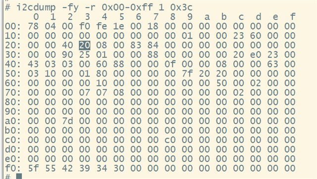
    If I don't use the strap pin to configure, how to configure it by registers? I tried reg23=0x20, but it couldn't capture the image.

    Below is the configuration when MODE_SEL0 and MODE_ SEL1 pulled down.

    And this is the configuration by registers:

    Best regards

    kailyn

  • Hello Kailyn,

    Let me go through this and get back to you.

  • In the pattern configuration mentioned above, if the total horizontal line width is changed from 1360 to 1350, the image cannot be captured correctly; so adjust the timing of the actual image, HBP = 32,HT = 1360, Hspw=32, VBP = 32, VT = 800,VSPW=32, images can be captured correctly, why?

    This is nothing related to our device. Our device doesn't care about the resolution sent. It just forwards the data. So, they need to check the settings on the SoC .

    If I don't use the strap pin to configure, how to configure it by registers? I tried reg23=0x20, but it couldn't capture the image.

    You are using a single lane SER, so I recommend you Strap the 940 into the correct mode instead of overriding this via registers.

    It looks like your register configurations are not correct. If you see reg 0x37 you find different values. For strap you have 0x88, and for register configs you have 0xFF which means different starp configs.