This thread has been locked.

If you have a related question, please click the "Ask a related question" button in the top right corner. The newly created question will be automatically linked to this question.

DS15BR401: LVDS output overshoot

Part Number: DS15BR401

Hi BU friends,

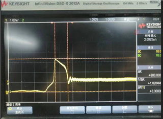
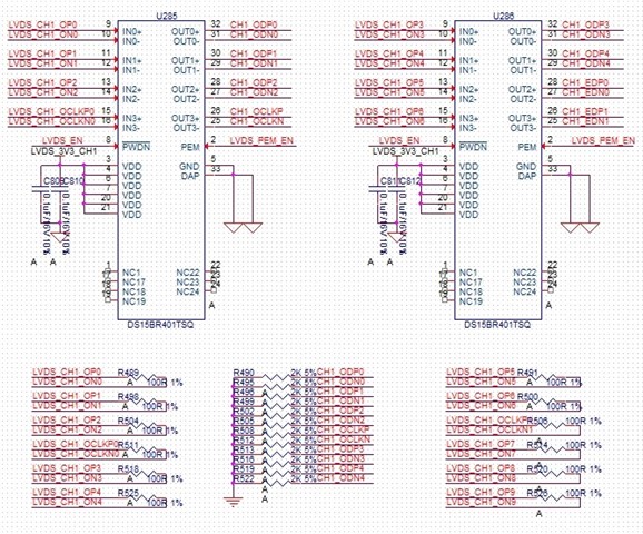
My customer used DS15BR401TSQ and met the LVDS overshot. Here is the waveform of the device. The Green wave is LVDS and the yellow is PWDN. And the LVDS output connected device has internal 100ohm termination resistance. Could you please give some suggestion. Thanks for your help!
  • Greetings,

    1). Please note figure 2 of the DS15BR401 data sheet. This part requires external 100-ohm termination on its input. This part has integrated internal 100-ohm termination.

    2). Similarly, please note figure figure 14. On the left hand side, this could be DS15BR401 with its integrated 100-ohm output termination. While on the right this could be DS15BR401 with external 100-phm termination.

    3). Please confirm differential LVDS trace is 100-ohm impedance controlled. Ringing and overshoot indicates impedance mis-match.

    Regards,Nasser  

  • hi  expert,

    I confrim differential lvds trace is 100 -ohm impedance controlled.

    For the one  LVDS overshot ,I don't think it's Ringing,  if something else caused the promblem ,Could you please give some suggestion?

  • Scope shot shows this is inductive and then there is some sort of RC time constant. Suggestion is to do TDR. I believe there is some impedance discontinuity through  the signal path.

    Regards,Nasser

  • hi  expert,

    1. The LVDS overshot reaches 3.3V,

    2.A load discharge pull down path can be used on either output (1 kΩ to ground recommended) ,Now customer use 2 KΩ to g ground ,What is the range of resistance to the ground?

    3.String 100Ω resistance at the 401 output end, but the waveform does not change,

    Could you please give some suggestion?

  • Hi Ian,

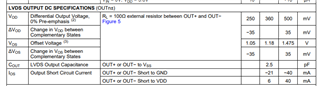
    Please note data sheet LVDS output parametric table below. With ~1.2V common mode voltage and 350mV differential output, signal should swing around 1.2V common mode voltage with 175mV mv swing. Given it overshoots to 3.3V, it means there is some component that is pulling this output to 3.3V. Please note figure 5 & 6 of the data sheet and recreate this setup. It might be a good idea to use a fresh part in a case device has been damaged by pulling output signal to 3.3V.

    Regards,Nasser

  • hi  expert,

    The customer uses six DS15BR401 boards,All it is overshot to 3.3V, Whether there is a hardware design source file for reference?

  • Hi Ian,

    This is a legacy old mature product and there is not a reference schematic or design. 

    One idea, customer can consider DS25CP104. This device has reference design and it has small cross point functionality. Please recommend this to your customer. Here is a link to this parts product folder:

    https://www.ti.com/product/DS25CP104A?keyMatch=DS25CP104A&tisearch=search-everything&usecase=GPN#design-development

    Regards,Nasser