This thread has been locked.

If you have a related question, please click the "Ask a related question" button in the top right corner. The newly created question will be automatically linked to this question.

MAX3221: About layout guideline

Part Number: MAX3221

Hi team.

My customer is designing the layout for MAX3221.

I guess they have to care about below:

  • Parallel and equal length wiring for the Dout Rin.
  • For DIN and Rout, creepage distance should be secured atleast twice the line width, and equal length routing is not preferred
  • Line width is not specified.

Is there any other tips for the layout guideline to reduce niose?

It will help if there are some collaterals that explains some tips for the layout for this device.

Regards,

Ohashi

  • RS-232 signals are slow and have low currents. This device limits the slew rate to less than 30 V/µs. So there are no special requirements for the Din/Dout/Rin/Rout signals. (The signals are not differential, so parallel or equal-length routing does not make sense.)

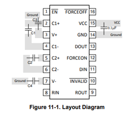
    The charge pumps generate high-current spikes; the traces to all capacitors should be as short and wide as possible (see section 11.1).

  • Ohashi,

    To add on to what Clemens has already given, I can lead the customer to page 15 of the datasheet where is shows a layout diagram. 

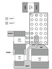
    The basic idea is to keep the charge pump and decoupling capacitors close to the pins, as well as have large pour areas to ensure adequate current flow. Here is a more in-depth example of what I am talking about from another application note (not specific to the MAX3221 - this is a PCB layout of another device - don't copy exactly)

    This shows a little more detail on how the polygons are designed to include the entire pad area of the capacitors. 

    • Parallel and equal length wiring for the Dout Rin.
    • For DIN and Rout, creepage distance should be secured atleast twice the line width, and equal length routing is not preferred
    • Line width is not specified.

    I believe maximum recommended data rate is 250kbps. Parallel and equal length wiring is not necessary for Dout/Rin, but looks neat on a PCB. 

    Footprint pads on the TSSOP package drawing are about 0.45mm = ~17.71 mils. For DIN and ROUT, 10 mil traces would work. Minimum distance between them is usually dependent on the PCB manufacturer. I am assuming there are no groves in the pcb when calculating creepage distance? Is there any reason for such a large trace width gap? If 2 x the line width is required, use < 10 mils for DIN/ROUT traces.