This thread has been locked.

If you have a related question, please click the "Ask a related question" button in the top right corner. The newly created question will be automatically linked to this question.

SN65DSI84: Flickering issue

Part Number: SN65DSI84
Other Parts Discussed in Thread: DSI-TUNER,

Hi,

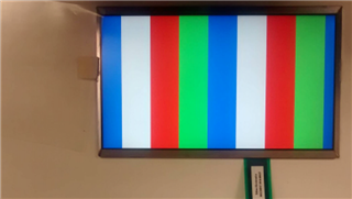
I have a flickering issue with my LVDS LCD panel

I follow the datasheet about sequence initilization and the DSI tuner to configure all the registers

Unfortunately, I still have the flickering issue 

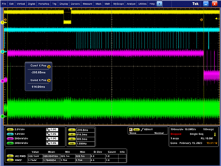
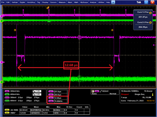
I took screenshot about LVDS and DSI sync
  • Picture, 36:
CH3 = LVDS_DATA0
CH4 = DSI_CLK
  • Picture, 37 to 39
CH3 = LVDS_DATA0
CH4 = DSI_DATA0
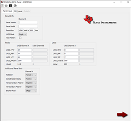
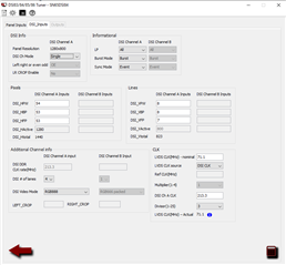
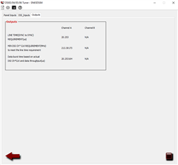
Also with the DSI tuner software, I filled in the fields based on our panel datasheet (attached our datasheet).
Did I fill it correctly?
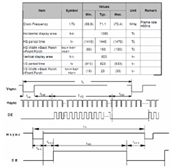
LCD Panel datasheet extract :
Than you for your response
  • Hello, Charles,

    Last time we chatted I provided the links below and provided some inputs onto how the original scope shots initialization sequence that was not being followed.

    https://e2e.ti.com/support/interface-group/interface/f/interface-forum/852871/faq-sn65dsi84-no-display-output-with-sn65dsi83-sn65dsi84-sn65dsi85

    Could you please send the scope shot with the enable pin going high and the DSI_DATA0 and DSI_CLK so that I can verify the initialization sequence?

    Have you also verified that the line time on the DSI input is meeting the line time on the LVDS output?

    As shown here for reference: https://e2e.ti.com/support/interface-group/interface/f/interface-forum/990480/faq-sn65dsi84-how-to-debug-flickering-video-with-sn65dsi83-sn65dsi84-and-sn65dsi85

    Upon assessing the DSI-Tuner snippets that you sent, I don't quite follow why the LVDS_HFP is not the same as the DSI_HFP. This could be why the outputs snippet is giving a line time mismatch estimate which could result in flickering. Could you please verify the DSI_HFP and LVDS_HFP?

    Thanks,

    Zach

  • Hello Zach,

    Yes sorry, I forgot to attach it

    Please, find below our new sequence:

    CH1=ENABLE

    CH2=I2C_SCL

    CH3=DSI_DATA

    CH4=DSI_CLK

    And I wrote the wrong number, below the right settings:

    Thanks,
    Charles

  • Hi, Charles,

    I don't immediately see anything wrong with your configuration. However, I am curious why you have the device EN = HIGH then pull low and then high again. The first time you are in EN = HIGH the DSI data is not in the LP11 state.

    First, could you try to configure the device to output only the internal test pattern like below?

    You can also configure the device to output an internal test pattern using the DSI-Tuner. When configured for the test pattern, the device does not use the input DSI data. It only uses the DSI CLK or an external REFCLK to internally generate a test pattern based on the LVDS timing parameters. The test pattern looks like the below:

    If the test pattern looks exactly like above, then any flickering seen when DSI data is used is likely due to an unstable DSI input or incorrect output from the DSI source. If there is flickering or incorrect color with the test pattern (e.g. the white strip appears gray) then the LVDS output has likely not been configured correctly for the display panel. Check that you’re using the correct format (Format 1 vs. Format 2) for the display panel, and that the LVDS timing is within spec.

    Have you also verified that the line time on the DSI input is meeting the line time on the LVDS output?

    As shown here for reference: https://e2e.ti.com/support/interface-group/interface/f/interface-forum/990480/faq-sn65dsi84-how-to-debug-flickering-video-with-sn65dsi83-sn65dsi84-and-sn65dsi85

    Thanks,

    Zach

  • Hi Zach,

    About the EN pin, it is because there is an internal pull-up in the SN65DSI84 chip.
    So, when we power-up the board, the pin goes from low to high and stay high until the CPU intializes the DSI sequence.

    Is it the wrong way to do ?

    We will do the pattern test and come back to you with the results.

    What do you mean exactly about line time on DSI and LVDS ?

    Is it that measure below ? Should it be equal/less/more than DSI tuner result ? (~20µs)

    Best regards,

    Charles

  • Charles, 

    Also, I found one more problem with your DSI Tuner tool after looking at your panel specs. You need to be using Format 2 not Format 1. To verify, you can compare the panel's datasheet section 3.3.3 to the DSI84's datasheet Figure 7-5. Flatlink Output Data (Format 2); Dual-Link 24 Bpp

    The need is for the DSI and LVDS line time to match. The line time on the LVDS output is the total amount of horizontal pixels divided by the LVDS clock frequency. You can measure the line time on the DSI input with an oscilloscope by zooming in on the data stream on of the data lanes like the measurement you are showing above. However, it looks like the measurement you are showing above is for the LVDS_DATA0. You would need to compare this to the DSI_DATA0.

    Thanks,

    Zach

  • Zach,

    We use only 1 LVDS channel, not 2. So why do I need to choose the FORMAT 2 ? (0x18=0x7A)

    We changed the values of registers and we got the good pattern

    registers        values

    0x20              0x20
    0x21              0x03
    0x24              0x00
    0x25              0x05
    0x2C              0x05
    0x2D              0x00
    0x30              0x36
    0x31              0x00
    0x34              0x0F
    0x36              0x35
    0x38              0x0F
    0x3A              0x35
    0x3C              0x10

    But we still have the flickering issue ....

  • Hello, Charles,

    Format 2 does not have to do with the number of links but rather the order of the bits. In data Format 2, the two MSB per color are transferred on the Y3P/N LVDS lane as shown in the picture of the devices data sheet. You can ignore the B channel since as you pointed out you are only using the A channel.

    Thanks,

    Zach

  • Hi Zach,

    Thank you for your reply and I understand  better now.

    So we did some test pattern and we got the right color but we have the last pixel line who do "flickering". The last line is not stable

    Do you have an idea to fix it ?

    Thanks,
    Charles

    Moreover, 

  • Hello, Charles,

    Are you saying that you are using the internal test pattern and you get some flickering or discoloration?

    If so, the flickering or incorrect color with the test pattern (e.g. the white strip appears gray) then the LVDS output has likely not been configured correctly for the display panel. Check that you’re using the correct format (Format 1 vs. Format 2) for the display panel, and that the LVDS timing is within spec.

    First, I was looking back at your datasheet for this application and noticed that your HSYNC and VSYNC polarities need to be set as POSITIVE and not NEGATIVE as you show is the DSI-Tuner. 

    Second, have you measured the LVDS clock and could you verify that what you are setting in the DSI-Tuner tool is actually the frequency being output by the device?

    Lastly, after trying #1 and #2, you could try adjusting the LVDS clock to see what impact that may have on the screen.

    Thanks,

    Zach

  • Hi Zach,

    Not the test Pattern, the screenshot comes from our normal mode. (the pixel of the very last line is flickering)

    I configured the register 0X18=0x7C (FORMAT2, 24bpp), I could test with the value 0x0C

    Yes,  I measured the LVDS clock, we got 72MHz (The LCD datasheet shows a range between : 68.9MHz and 73.4MHz

    One more thing, I use the spread spectrum on DSI clk , is it okay for the bridge ? (In the datasheet, it seems okay)

    Thanks,

    Charles

  • Charles,

    Please perform the following:

    1. You still need to use the HSYNC and VSYNC polarities = POSITIVE and NEGATIVE as you show is the DSI-Tuner. Per the panel's datasheet both the HSYNC and VSYNC are driven high as the DE is driven high.

    2. Could you try the internal test pattern to see if there is flickering? If there is no flickering this will help narrow down the issues to the DSI data stream.

    3. Please verify that the video timing output from your DSI source matches what you are programming into the DSI83/DSI84/DSI85. This includes the DSI CLK frequency, active pixel data, and blanking pixel data.

    4. Could you measure the DSI_DATA0 line time?

    Thanks,
    Zach

  • Hi Zach,

    I tried to perform your 4 steps:

    1. It is okay : HSYNC = NEGATIVE / VSYNC = NEGATIVE / DE = POSITIVE

    2. There is no flickering with internal test pattern

    3. 

    With the spread spectrum on DSI clock, we have a frequency  focus on 216MHz, so we configured the register with 0x12=0x2B

    4. On osciloscope, I measured DSI_DATA0 line time, I got = 11.6µs

    And with the formula for DSI : Line time = (Htotal * bpp) / (2 * # of DSI DataLanes * DSICLK) =  (835*24) / (2*4*216MHz) = 11,6µs (Ref : "Troubleshooting SN65DSI8x - Tips and Tricks")

    And for LVDS : Line Time = Htotal / LVDSCLK = 835 / 72MHz = 11,6µs

    Do you know if the spread spectrum function on DSICLK is a good choice ?

    Thanks,

    Charles

  • Hello, Charles, 

    Since the internal test pattern test pattern has no flickering then the flickering seen when DSI data is used is likely due to an unstable DSI input or incorrect output from the DSI source.

    Spread spectrum clocking (SSC as it is shown in the datasheet) is best for applications where EMI is of concern but SSC will add some jitter to your clock.

    Looking at your histogram I see that you spread the spectrum quite wide. The spectrum should be typically a 1% spread. For your clock this is about 213.84 MHz to 218.16 MHz.

    Thanks,

    Zach

  • Hi Zach,

    Thank you for your reply

    There is no flickering with our internal test pattern. However, could you please tell me what register I need to configure ? To be sure to do the right things.

    Now we sent those registers:

    i2cset -y -f 2 0x2C 0x20              0x20

    i2cset -y -f 2 0x2C 0x21              0x03

    i2cset -y -f 2 0x2C 0x24              0x00

    i2cset -y -f 2 0x2C 0x25              0x05

    i2cset -y -f 2 0x2C 0x2C              0x0A

    i2cset -y -f 2 0x2C 0x2D              0x00

    i2cset -y -f 2 0x2C 0x30              0x36

    i2cset -y -f 2 0x2C 0x31              0x00

    i2cset -y -f 2 0x2C 0x34              0x0F

    i2cset -y -f 2 0x2C 0x36              0x35

    i2cset -y -f 2 0x2C 0x38              0x0F

    i2cset -y -f 2 0x2C 0x3A              0x35

    i2cset -y -f 2 0x2c 0x3C              0x10

    However, when we send next, the register 0x18 = 0x1A or 1C, the strip is white with 1A and grey with 1C.
    But, when write (at the init sequence) 0x18=0x1A the screen has the wrong color but with 1C it has the right color

    Our Register configuration:

    09 = 00
    0A = 05
    0B = 10
    0D = 00
    10 = 26
    11 = 00
    12 = 2B
    13 = 00
    18 = 1A
    19 = 0A
    1A = 00
    1B = 33
    20 = 20
    21 = 03
    22 = 00
    23 = 00
    24 = 00
    25 = 05
    26 = 00
    27 = 30
    28 = 21
    29 = 00
    2A = 00
    2B = 00
    2C = 0A
    2D = 00
    2E = 00
    2F = 00
    30 = 36
    31 = 00
    32 = 00
    33 = 00
    34 = 0F
    35 = 00
    36 = 35
    37 = 00
    38 = 0F
    39 = 00
    3A = 35
    3B = 00
    3C = 00
    3D = 00
    3E = 00
    0D = 01
    09 = 01

    With that configuration, there are still flickering, do you have any advice ? Do I need to change something ?

    Thanks,
    Charles

  • Hello, Charles,

    If there is flickering or incorrect color with the test pattern (e.g. the white strip appears gray) then the LVDS output has likely not been configured correctly for the display panel. Check that you’re using the correct format (Format 1 vs. Format 2) for the display panel, and that the LVDS timing is within spec.

    Based on what I said above you are outside maximum spread of the spectrum with the DSI CLK. The spectrum should be typically a 1% spread and maximum 2%. You need to be within about 213.84 MHz to 218.16 MHz.

    Thanks,

    Zach

  • Hello Zach,

    Effectively, we are outside, we try to reduce or disable the spread spectrum.

    However, on internal test pattern, we didn't see flickering.
    If we don't see flickering on internal test pattern, we sould don't see flikcering on normal mode, right ?

    About FORMAT 1 vs FORMAT 2, below our LCD specification (shortly):

    • 24bpp
    • MSB on lane 3
    • Single-Link

    What I can see on SN65DSI84 datasheet, for an LVDS output with config : 24bpp and MSB on lane 3, there is only a dual-link possibility ...

    So Do I need to configure the output on dual-link and send twice the picture (2x (800x1280) pixels)? Or that is only an illustration ?

    Thank you,

    Charles

  • Charles,

    Let me recap what we have so far from our troubleshooting:

    - We've checked that you are configuring the device correctly using the DSI-Tuner 

    - We've checked that the LVDS timing parameters (clock frequency, etc.) are within specification of your display panel.

    - Verified that you are getting the internal test pattern as shown below:

    - You checked the burst/line time on the DSI input. You made sure the line time (time from HSYNC to HSYNC) on the DSI input matches the line time on the LVDS output.

    From this we've narrowed down the possible causes for the flickering:

    Since the test pattern looks exactly like above, then any flickering seen when DSI data is used is likely due to an unstable DSI input or incorrect output from the DSI source.

    Since you are using a spread spectrum clocking, the DSI clock can still be an issue since clock jitter can be an issue if the line time matches.

    You can also try using a clean external REFCLK as the clock source for the PLL instead of using the DSI CLK as the PLL source, as an excessively noisy DSI CLK may lead to an unstable LVDS clock output.

    Thanks,

    Zach

  • Zach,

    We are trying to use external clock REFCLK, I let you know if we fix the issue

    Are there something to configure in particulary in order to use REFCLK ? Only register 0x0A.0 and 0x0B.1:0 (Multiplier equal 1, because REFCLK = 72MHz)

    Best regards,

    Charles

  • Zach,

    We tried, and we still have flickering

    However, I checked the datasheet of the oscillator and it is written rise and fall time 3ns maximum ... I checked on the oscillo and I got a rise and fall time between 2ns and 3ns

    Based on the datasheet of SN54DSI84, the rise and fall time must be between 100ps and 1ns

    Do I need to change the ref of oscillator ? Or Do I need to change something else with the registers ?

    The internal test pattern is clean

    Line time of DSI data : 11,56µs

    Line time of LVDS : Horizontal total / F_LVDS = 834 / 72 MHz = 11,58MHz

    Registers : 0x0A = 0x04 / 0x0B = 0x00 

    Thanks,

    Charles

  • Charles,

    The REFCLK must meet the requirements as listed in the DSI84 datasheet.

    Please follow section 7.3.1 Clock Configurations and Multipliers to configure your clock. You can use the DSI-TUNER tool as well to assist you.

    From 0x0A you have 010 – 62.5 MHz ≤ LVDS_CLK < 87.5 MHz as a REF_CLK enabled

    0x0B is set to LVDS clock = source clock (default)

    Thanks,

    Zach