Because of the holidays, TI E2E™ design support forum responses will be delayed from Dec. 25 through Jan. 2. Thank you for your patience.

This thread has been locked.

If you have a related question, please click the "Ask a related question" button in the top right corner. The newly created question will be automatically linked to this question.

SN65HVD72EVM: Strange differential waveform

Part Number: SN65HVD72EVM
Other Parts Discussed in Thread: SN65HVD72

Hi Team,

Now I am conducting test on sn65hvd72EVM with sn65hvd72 soldered, finding the measured differential waveform is quite strange.

Two boards are connected together for simulating real transmission : One for sending and the other for receiving.

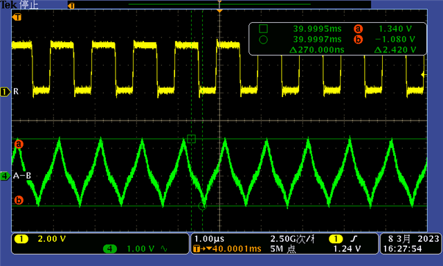
When sent data is 1MHz square waveform with 0V-3V, the measured differential waveform and receiving waveform are shown below:
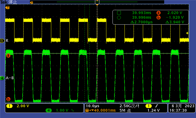
And when send data is 100kHz square waveform with 0V-3V, measured waveforms are shown below:
I have several questions about waveforms:

1. Why the differential waveform is not square when sent data is 1MHz?

2. Why the part could output 1MHz square waveform in receiver? Since sn65hvd72 could only support 250kps.

3. Why the amplitude varies with frequency?

BRs

Zixu

  • 1. The slew rate is limited to reduce EMI.

    2. A propagation delay of 75 ns is enough to handle 1 Mbps.

    3. Due to the limited slew rate, the voltage does not reach the final value before the signal reverses.

  • Hi Zixu,

    1. This device is slew rate limited to reduce EMI - its not a square wave because higher frequency content is being filtered out - so the fast transitions are removed from the output.

    2. As Clemens said - the propagation delay on the receiver can support 1Mbps  - but the driver cannot so the driver is the limiting factor for data rate on the device.

    3. Due to the slew rate limiting - the voltage doesn't have enough time to reach its full value before reversal.

    Best,

    Parker Dodson

  • Hi Parker,

    Thanks for your answer. But it is still a confusing point that how could sn65hvd72 convert distorted differential waveform to normal square waveform in receiver terminal under 1MHz?

    BRs

    Zixu

  • The receiver requires a differential input voltage of no more than 50 mV to 180 mV to switch, and uses hysteresis. RS-485 is designed to work in very noisy environments.

  • Hi Zixu,

    This is due to a few reasons:

    1. The driver outputs are slew rate limited - but the receiver outputs are not. 

    Driver transition time (fall or rise time): 300ns (min), 700ns(typ), 1.2us(max) (54 Ohm || 50pF Load) 

    So when applying a 1MHz signal the output will be slew rate limited (essentailly the conversion from square wave to triangle wave as seen in your tests)

    The bit time for a 1MHz signal (1Mhz is 2Mbps  - as 2 bits can be sent per cycle) The bit time in that situation is 500ns - the typical transition time for the driver is 700ns so the driver will not be able to achieve its full value.

    The typical propagation delay is 700ns so you could even lose bits by applying a 1MHz signal (2Mbps) - if you mean a 1Mbps signal (500KHz) the propagation delay may not be as much of an issue but the transition time will still be an issue.

    The receiver transition time (fall or rise time): 12ns (typical),30ns (max) (15pF load) - so the transition time is going to be much shorter than the bit time allowing for the output to come to a square wave.

    The receiver also has a propagation delay of 75ns to 100ns (typical and max with 15pF load) which is less than the bit time so it that won't be limited there either. 

    2. The differential receiver inputs have low value thresholds.

    The voltage between A and B have a positive going threshold max of -20mV and a minimum negative going threshold -200mV - so if the signal has a maximum of > -20mV and a minimum of < -200mV the device will receive a valid logic level.

    When you take both of these facts + the tests you have done:

    1. The triangle wave is formed due to slew rate limited driver outputs - this forces a slower rise and fall time and due the speed of the input signal the full value isn't reached and a triangle wave is formed.

    2. The triangle wave positive peak is > -20mV and the negative peak is <-200mV so the receiver is reading valid logic levels.

    3. The receiver propagation delay and transition times will allow a 1MHz square wave generation at the output. when valid logic levels are reached.

    Please let me know if you have any other questions!

    Best,

    Parker Dodson