Part Number: DS25BR150
Other Parts Discussed in Thread: TLV3801, , DS25CP152
Hello,
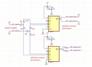
We're using TLV3801 https://www.ti.com/lit/ds/symlink/tlv3801.pdf in our application and we're looking to split its LVDS output such that one goes to FPGA and the other goes to an SMA port for connecting to a scope. Please find circuit attached below. We're looking to use an LVDS buffer on each of the two split branches to maintain signal integrity and have found DS25BR150 https://www.ti.com/lit/ds/symlink/ds25br150.pdf to be a suitable part for this. Since DS25BR150 is internally 100 Ohm terminated, is the circuit shown below a good solution to achieve the split?
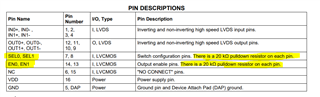
Each transmitter and receiver have an impedance of 100 Ohm. Analyzing the upper branch we start with that 100 Ohm, when we add R2 and R4 the impedance of that branch is 133 Ohm. The two receiver branches in parallel have an impedance of 66.5 Ohm. Last, we add the 33 Ohm from the two series resistors from the transmit branch, R1 and R5 for a total of 99.5 Ohm as seen from the transmitter output. The analysis is the same for each of the branches so each DS25BR150 will see a 100 Ohm load.
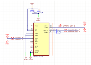
The upper branch DS25BR150 output goes to FPGA and the lower branch output is AC coupled and goes to an SMA port.