Part Number: SN75DP139
Hi Sir,
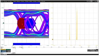
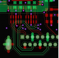
may we know this differential input layout is correct?
D0/D1/D2/CLK(D4) will have two pairs of wires that need to be routed through the VIA layer and bypass the DIP pin connector.
Therefore, each pair of D0/D1/D2/CLK lines is not equal in length.