Part Number: SN65DP159
Hi,
I will use the SN65DP159 for HDMI Input Interface to a Xilinx MPSoC FPGA.
The TMDS Data comes from a Sony Camera.
The camera do not support an I2C Interface.
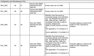
I found the following note in the SN65DP159 datasheet:
Note 1: For applications where the GPU or Sink does not support clock stretching the DDC lines from the GPU/DP TX
should bypass the SCL_SRC and SDA_SRC but still connect to the SCL_SNK and SDA_SNK pins on the DP159.
The SCL_SRC and SDA_SRC pins must be pulled to ground. Note that if the GPU/DP TX cannot support the 5V
DDC lines from the connector, a level shifter is needed to step down the 5V signals to the voltage level the GPU/DP
TX can support.
If I understand this correctly the I2C_SRC interface has to pulled to GND and the I2C_SNK Interface has to be left unconnected.
Is this correct?
Thanks,
Patrick