Other Parts Discussed in Thread: TDP1204
Hello,
Dear TI Technical Support,
I have a question about as a title, TDP0604 DP++, HDMI Level shifter,especialy DDC level shifter.
Now I have a problem with DDC. When using DP++ to DVI applications.
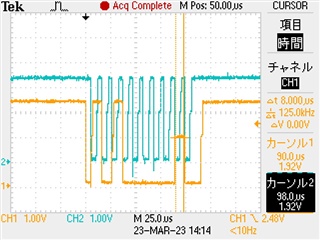
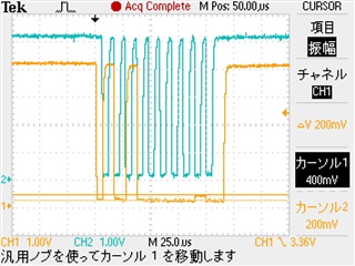
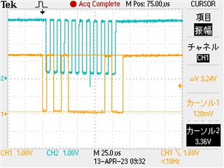
I saw the TDP0604 returning a NAK-like signal (1.7V-HIGH) on DDC_SDA on the LV side.
However, the HIGH level of the LV side common was 3.3V.
Q1. Was it due to a signal collision or something?
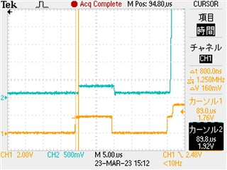
In this application, the master device(LV 3.3V side) has a internal 100KΩ pull-down for SCL and a 100KΩ pull-up for SDA.
Q2.Could this be a problem?
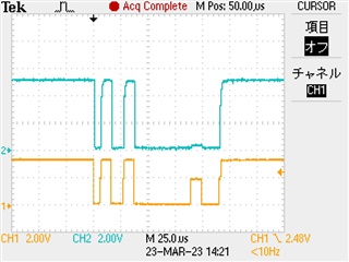
When the MODE pin is disabled, LV_DDC_SDA will return a NAK signal at 3.3V-HIGH.
Q3.Is this circuit berow correct?
With DDC disabled on the MODE pin
and bypassing the DDC level shift with another discrete IC
(with situation stil connected to both of TDP0604 DDC level shifter pin which HV and LV side),
DDC can now be read by master device and Master device can TMDS video output.
or Must be left open HV side or LV side as a datasheet Figure 8-6 or Figure 8-7?
Thank you read this question.
I hope your reply.
Best Regards,
Yuji Masita.