This thread has been locked.

If you have a related question, please click the "Ask a related question" button in the top right corner. The newly created question will be automatically linked to this question.

TCAN4550-Q1: delay compensation setting

Part Number: TCAN4550-Q1
Other Parts Discussed in Thread: TCAN4550

Hi team,

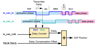
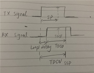
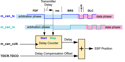
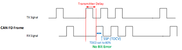
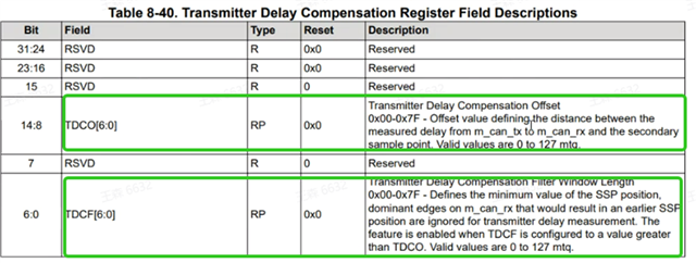
Customer has found some fault frame issue in project and they'd like to adjust the delay compensation register to fix it. Could you help share

1. if any guideline to set below TDCO and TDCF register?

2. how long is mtq?

3. what's the relationship between TDCO, TDCF and TDCV

*Use external 40M crystal oscillator

thank you

Scarlett

  • Hi Scarlett,

    1. if any guideline to set below TDCO and TDCF register?

    Generally the TDCO and TDCF register values should be set to match the DTSEG1 value used.  Note that the DTSEG1 register value is interpreted as 1 more than the actual value because a value of 0 is not allowed.  However the TDCO and TDCF register values are not interpreted as 1 more than the actual value.

    2. how long is mtq?

    A Minimum Time Quantum (mtq) is equal to one period of the CAN clock.  If a 40MHz crystal is used, then 1mtq = 25ns.

    A Time Quantum (tq) can equal some multiple of mtq and is dependent on the Bit Rate Prescaler (BRP) that is used when defining the bit timing.  If a BRP of 1 is used, then 1tq = 1mtq.  However, if BRP=2, then 1tq = 2mtq, etc.

    The TDCO and TDCF are always configured in terms of mtq.  Therefore, if the BRP = 1, then the TDCO and TDCF settings can be set to the same number of tq as the DTSEG1 (or one value higher than DTSEG1 since the DTSEG1 is interpreted as 1 greater than the actual value).  However, if the BRP is > 1, then the appropriate number of mtq must be calculated to equal the DTSEG1 tq.

    3. what's the relationship between TDCO, TDCF and TDCV

    The TCAN4550-Q1 uses the MCAN CAN FD Controller IP developed by Bosch, and I would refer you to the MCAN User's Manual for more detailed information on the features of the MCAN controller.

    Section 3.1.4 of the MCAN User's Manual discussed the details of the Transmitter Delay Compensation circuit and how to configure it to create the desired Secondary Sample Point (SSP).

    The Transmitter Delay Compensation consists of the sum of two different delay values.  The first delay value is the actual transmitter loop delay and is measured by the device on each transmitted CAN FD frame at the falling edge of the FDF bit to the res bit.  This aligns the beginning of the TX bit and the RX bits by removing the loop delay.

    The second delay is set by the TDCO mtq configured in the register value.  In terms of the SSP, the TDCO value is equivalent to the number of tq before the SSP which is essentially the same as the DTSEG1 value in the Data Bit Timing and Prescaler (DBTP) register.  This is why we usually set the TDCO to the same value as DTSEG1.

    The actual Transmitter Delay Compensation Value (TDCV) is the sum of the loop delay and the TDCO.

    The Transmitter Delay Compensation Filter (TDCF) window defines the minimum value for the SSP position.  This value is to prevent noise or glitches from being interpreted as valid bit transition during the FDF to res bit delay measurement that could lead to early SSP positions.  This is essentially the minimum value of TDCV (or delay time + TDCO). 

    If the TDCV (or delay time + TDCO) is < TDCF, then the SSP will be equal to the TDCF value.  However, if the TDCV (or delay time + TDCO) is > TDCF, the SSP will be equal to the TDCV (or delay time + TDCO).

    Generally we would want the TDCF to be as close to but not greater than the TDCV (or delay time + TDCO) to ensure the SSP is always at the TDCV value.  However, we don't always know what the delay time is and it could fluctuate a little based on external factors, so it is recommended to set the value of TDCF to be equal to TDCO.  This value could be adjusted if the delay time is known, or there are some observed bit errors that could be removed from a longer filter window.

    So as a summary and general recommendation, the DTSEG1, TDCO and TDCF are all set to the same amount of tq (mtq).  This should establish a good basic communication that can be refined and adjusted for each specific system.

    Regards,

    Jonathan

  • Hi Jonathan,

    Thanks for your very detailed reply.  Do you have any comment on if CAN FD cable length has any relationship wth SSP and how to adjust SSP?

    Thank you

    Scarlett

  • Hi Scarlett,

    The cable length could be a factor that needs to be considered because longer cables can create longer loop delays and create more "ringing" from a dominant to recessive transition that must subside before sampling the bit. 

    The device will automatically measure the loop delay but the ringing will require the sample point to be shifted towards the end of the bit to allow time for the signal to stabilize.  But this is no different than the considerations that need to be made with regards to receiving data transmitted by other nodes.

    So I would say that in this respect there is not fundamental difference when adjusting the SSP and the normal bit timing sample point (SP).

    To make adjustments to the SSP, start by setting the TDCO and TDCF to be equivalent to the DTSEG1 value which is the number of time quantum before the sample point (SP).  Note, it is generally recommended to have a sample point of 80%.  Then adjustments can be made to either increase the TDCO, TDCF, and DTSEG1/DTSEG2 values to refine the SP and SSP locations while monitoring the Transmitter and Receiver Error Counters (TEC and REC). 

    Monitoring the CANH and CANL signals with an oscilloscope can also help determine if there is excessive ringing that needs to be avoided with a later SP and SSP %.

    Regards,

    Jonathan

  • Hi Jonathan, 

    For the CANFD 2M cable 3m length case, 

    1. When TDC is not enable:

    a) When loop delay shorter than 400ns, SP set to 80% sample point, can still get RX signal

    b)  When loop delay longer than 400ns ,80% SP cannot be covered, will report fault frame?

    2. When TDC is enable

    a) When loop delay shorter than 400ns, SP set to 80% sample point, can still get RX signal

    b) When loop delay longer than 400ns, because TCAN4550 has enable TDC, TCAN4550 can automatically detect TX RX loop delay. SSP set to 80% or TDCO 16mtq is equal.? How to set TDCF TDCV?

    Thank you

    Scarlett

  • Hi Scarlett,

    It is recommended to enable TDC when using CAN FD communication for all bit rates. Without TDC, the bit rates are required to be slow enough that the loop delay and sample point occur before the transmitter has finished transmitting the bit in order to get a correct verification that the received data matches the transmitted data.  With faster CAN FD bit rates, the bit period becomes smaller and this RX to TX correlation cannot be guaranteed without TDC.

    With short loop delays and some bit rates you may still get successful communication with some bit rates, but with others you will get errors.

    CAN bit timing is set based on the concept of a Time Quantum (tq) which is a length of time equal to an integer number of clock cycles. Each bit period is made up of 4 or more tq and the sample point (SP) is created by allocating a number of tq before and after the SP.  The bit rate is set by the total number of tq used for the bit which determines the length of the bit period and therefore the bit rate or frequency.

    A Minimum Time Quantum (mtq) is by definition the smallest length of time the device is able to work with and it is by definition equal to the length of time equal to one clock period.

    When a fast clock is used with a slow bit rate, there can be a lot of mtq's in the bit and sometimes it is desirable to work with a smaller number of tq's per bit.  In this case a prescaler can be applied to the clock to increase the number of clock cycles or mtq's per each tq.

    Therefore, when the prescaler = 1:

    1 tq = 1 mtq

    However, when the prescaler = 2:

    1 tq = 2 mtq

    The bit timing configuration is done in the Nominal Bit Timing and Prescaler )NBTP) and Data Bit Timing and Prescaler (DBTP) registers based on how many 'tq" are used for the bit and how many are located before and after the SP.  The prescaler used will determine how long each tq is.

    The Transmitter Delay Compensation registers only accept mtq for an input.  Therefore if the Data Bit Rate Prescaler (DBRP) is set to 1, 1 tq = 1 mtq and in your example, 16 mtq would equal 16 tq. But if your DBRP = 2, 16 mtq = 8 tq.

    It is recommended to set the TDCO and TDCF registers to the equivalent amount of time as the DTSEG1 register in the DBTP register.  Therefore you will need to convert the tq of the DTSEG1 register into an equivalent mtq based on the DBRP used.

    Also note, that the DTSEG1 interprets the value set in the register as 1 greater because a zero value is not allowed. But, a zero value is allowed for the TDCO and TDCF registers, so when setting these registers, you will need to make sure the "interpreted value of DTSEG1" and the TDCO and TDCF values have an equivalent number of mtq.

    The Transmitter Delay Compensation Value (TDCV) is calculated by the device and it can be read back.  It is just the sum total of the measured loop delay plus the TDCO value that has been configured.

    Regards,

    Jonathan

  • Hi Jonathan,

    Thanks a lot for your detailed reply.  I had some discussion with customer today, and we had some follow up question as below, looking forward to your feedback.

    1.  We want to confirm with you TDCV= Loop delay +TDCO, is our understanding as below figure correct?

    2.Our suggestion is to set TDCF to the same as TDCO, therefore SSP will take TDCV value ( loop delay + TDCO) always as loop delay is greater than 0. So what's the point of setting TDCF register bit if never use this filter function?

    3. When loop delay is very small (like above picture shows), both SP and SSP can sample valid value. We want to know if we enabled TDC and can sample valid signal at SP, will TCAN4550 keep on sample SSP as well? And which value it will take from the two samples?

    4. Is it always suggested to enable TDC, then why it is disabled by default? 

    Thank you

    Scarlett

  • Hi Scarlett,

    1.  We want to confirm with you TDCV= Loop delay +TDCO, is our understanding as below figure correct?

    Correct.

    2.Our suggestion is to set TDCF to the same as TDCO, therefore SSP will take TDCV value ( loop delay + TDCO) always as loop delay is greater than 0. So what's the point of setting TDCF register bit if never use this filter function?

    By setting the TDCF value to be equal to TDCO you are using the filter function to ensure the SSP is at least equal to the TDCO. 

    The loop delay is calculated for every transmitted frame by measuring the time between the falling edge of the FDF bit on the transmitted out and the falling edge of the FDF bit on the received input.

    In the case where there is a dominant glitch in the received input, or noise of some sort that can cause the voltage to transition prior to the actual falling edge of the FDF bit, the delay count will be smaller than the physical transceiver loop delay resulting in an early SSP. 

    In order to avoid this, the TDCF bit is set which defines the minimum SSP location thereby ignoring any early dominant edges that may be falsely detected based on noise.  The SSP is calculated to be the point which is at least TDCF and where the falling edge of the received FDF to res bit is observed.

    3. When loop delay is very small (like above picture shows), both SP and SSP can sample valid value. We want to know if we enabled TDC and can sample valid signal at SP, will TCAN4550 keep on sample SSP as well? And which value it will take from the two samples?

    If TDC is enabled, the RX bit will always be sampled at the SSP sample location because the SP is only used with data that is transmitted from a different transceiver on the CAN bus. 

    Remember, the purpose of the "Transmitter Delay Compensation" is in the name itself.  The CAN protocol for error detection requires the transmitting node to monitor the received data and compare the bits to the transmitted bits.  If it detects any bits that are received differently that where transmitted, it is required to transmit an error frame to alert the other nodes on the CAN bus that there was a transmission error and to discard the message because it had bad data.

    In order to remove the loop delay and align the received bit with the transmitted bit, the Transmitter Delay Compensation circuit is used to create a Secondary Sample Point (SSP) that is used solely for the purpose of checking the transmitted bits for errors.

    The Sample Point (SP) is only used for received bits transmitted from other nodes.  Because we want to make sure the bits are sampled after any ringing noise on bit has subsided, we set the SP to about 80% of the bit period.  This is usually results in the best performance and fewest bit errors.

    To keep with this practice, we also try to set the SSP to be at the same 80% location of the received bit that has been delayed by the TDC.  This is why we set the TDCO value to be equal to the DTSEG1 value.  In doing so, we set the same 80% sample point within the bit period because the device will automatically measure and remove the loop delay for us.

    However, IF and ONLY IF the loop delay measurement was too small, the Transmitter Delay Compensation Filter will ensure that at least the SSP will be equal to the TDCO value.  This will result in an earlier than normal sample point for the SSP, but it should still be within the bit period.

    4. Is it always suggested to enable TDC, then why it is disabled by default? 

    This is a good question and I don't know because the MCAN Controller IP was developed by Bosch and licensed to TI for use in this device.  We would have to ask Bosch why they chose to disable the TDC bit by default, even though it is always recommended for use with FD data rates.

    Regards,

    Jonathan

  • Hi Jonathan,

    Thanks a lot for your detailed and quick reply.

    I'd like to confirm with you on point3. Whether or not TDC is enabled, SP is always used to sample the transmitted bit from other nodes on the CAN BUS ( other node's TX?). When TDC not enabled, no SSP will be sampled on RX. If TDC is enabled, SSP will be sampled on RX to check the bit of error during transmission. Is my understanding correct? 

    Thank you

    Scarlett

  • Hi Scarlett,

    Your understanding is correct.

    Regards,

    Jonathan

  • Hi Jonathan,

    Customer is also asking for a diagram to show the relation between TDV=delay +TDO (like the one I drew, but not correct). My understanding is it is hard to draw, since delay is calculated based on the falling edge of FDF bit, and TDV is actually calculated for the rest data bit. Want to check with you if my understanding is correct? And if you could help share a drawing?

    Furthermore, is there any application note on TDC and SSP available? Customer also would like to share across team regarding the theory and how to configure through software across team.

    Thank you

    Scarlett

  • Hi Scarlett,

    This is a feature of the MCAN Controller IP developed by Bosch so I would recommend they refer to the diagram and description in section 3.1.4 of the MCAN User's Manual.  This section discusses the details of the Transmitter Delay Compensation circuit and how to configure it to create the desired Secondary Sample Point (SSP).

    Regards,

    Jonathan

  • Hi Jonathan,

    Can I use below two pictures to understand the TDCV (The first one took from MCAN doc, the second one is drawn by myself)? Thank you

    Thank you

    Scarlett

  • Hi Scarlett,

    Yes, your drawing looks correct.

    Regards,

    Jonathan