Part Number: SN65DP141
Hi,
Good Day.
My case: Notebook -> DisplayBoard cable -> SN65DP141 as input buffer IC, i.e. pins IN0_P, IN0_N ... IN3_P, IN3_N -> FPGA (i.e, SN65DP141's lines OUT0_P, OUT0_N ... OUT3_P, OUT3_N connected to FPGA).
Next, GPIO configuration mode (not I2C !).
My questions:
1. Pin EQ_Mode/ADD2 (pin 35). What should I select? Cable (because I have a 3m DP cable from notebook to SN65DP141)? Or trace (because I have short PCB traces from SN65DP141 to FPGA)?
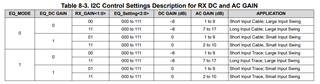
2. Pins EQ0/ADD0, EQ1/ADD1, RX_Gain. How should I select EQ_AC_Gain ? EQ_DC_Gain = 1 (or 0 dB) in my case.
Please advise. Thank you very much.
Best Regards,
Ray Vincent