This thread has been locked.

If you have a related question, please click the "Ask a related question" button in the top right corner. The newly created question will be automatically linked to this question.

TPD6E05U06: ESD

Part Number: TPD6E05U06
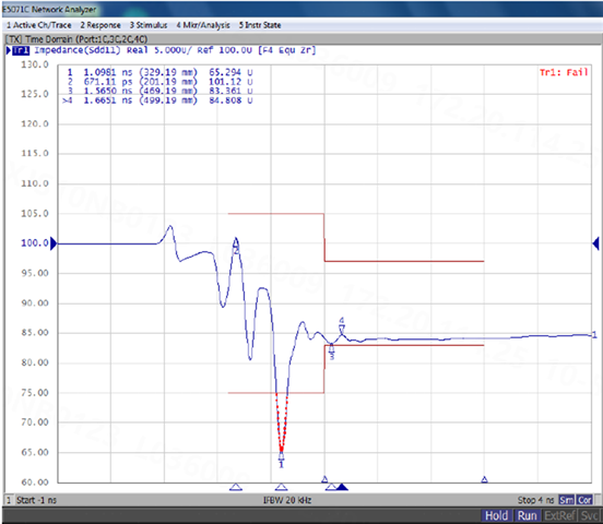
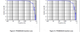
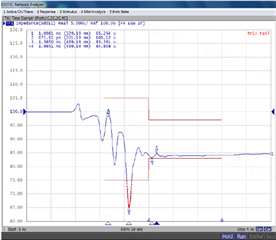
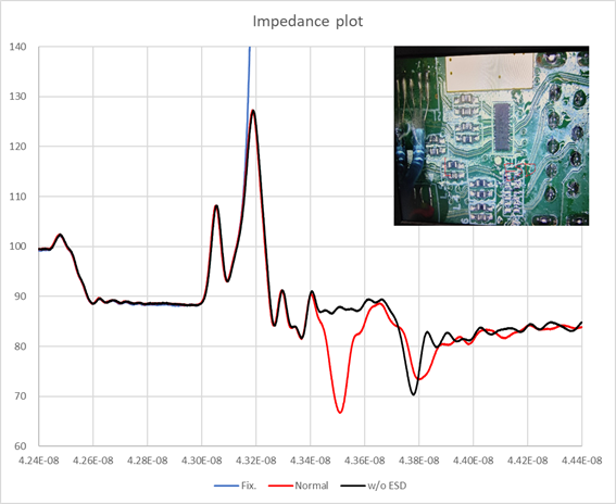
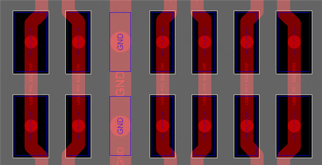
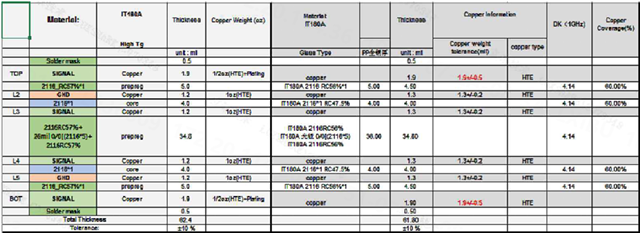
Customer feedback that the USB3.0 requirements cannot be met when using this product。
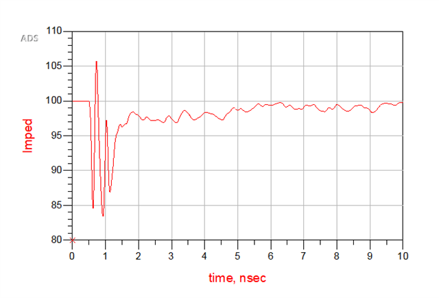
Do we have the related SI mode of high speed test?
Or any other experiment results?
Which could convince customers that this is not our device's problem.
  • Hi Fabio,

    We have eye diagrams of a 6 Gbps HDMI signal through this device: 

    USB3.0 should have a max data rate of 5Gbps so this device can definitely support that signal speed.

    Did the customer have issues with this device on their board?

    Many factors such as trace length and other components on the line will add capacitance that could bring the system out of compliance.

    Regards,

    Sebastian 

  • They just said; If no our device the test result is good.

    If our device on the board, it is bad and the impedance cannot meet the requirements of USB3.0, as the picture shows.

  • Is there any other material which could show to customers?

  • Adding the comment from customers:

    "Can you provide us with the SI model and test data? The specification includes testing high-frequency parameters. So there should be SI model and related test information."

  • Hi Fabio,

    The data provided clearly shows this device can support a signal that is 1Gbps faster than USB3.0. The eye diagram would be better with a slower speed signal.

    This data was taken on a board with optimized routing to minimize parisitics,if the board layout has high capacitance on the USB signal trace then this could be causing the system to move out of compliance.

    The insertion plot also shows this device has a differential insertion loss of -3dB at ~4Ghz (8Gbps). 

    There are IBIS and S-parameter models available on the product page. 

    Regards,

    Sebastian 

  • The customer focus on the impedance, not the diagram.

    1. Is the S model downloaded simulated or measured data?

    The abscissa of this data domain is a log model rather than a linear model. The impedance derived from this data is inaccurate, but it is clear that the impedance has a low point.


    2. Can you provide the linear S model or impedance test results (according to USB3.0 standard test results) shown in the following products (PN: TPD6E05U06RVZR)?
    Now they focus on impedance metrics, not eye diagrams or IL.

    3. The impedance specification of the USB3.0 association is 90+/-15 ohms. Therefore, if this requirement cannot be met, the product can be considered as substandard.

  • Hi, Sebastian Muriel

    Could you help to answer this question? Thanks

  • Hi Fabio,

    My apologies for the late reply I am on business travel.

    1. The S parameter model is created using simulated data

    2. We don't currently have a linear S model or impedance test results with this device. 

    3. It's impossible to avoid some impedance mismatching with ESD diodes protecting signals with frequencies in the ghz range. The device itself can support USB3.0 so that is not the issue,  the PCB layout must be optimized to minimize reflections. The trace lengths could be too long to be able to add TPD6E05U06 without moving the system out of compliance. Can you provide the layout? Also an image of the VNA waveform without the esd diode. 

    Regards,

    Sebastian 

  • The impedance plot below is the impedance comparison between the PCBA w ESD (red trace) and the one  w/o ESD (black trace).  It indicates that the PCB trace w/o ESD is about 90 ohms. The impedance drops about 20 ohms when the ESD attached.

    The picture below is the ESD footprint and the voids underneath it. As shown in the PCB stackup below, the PCB has 6 layers. The ESDs are attached on the bottom side.

    Except for optimizing the PCB layout, the customer also wants to know the impedance performance of the ESD itself. If the ESDs impedance is too low, the high impedance of the PCB can be pulled low by the ESD.

  • Hi Fabio,

    A lower capacitance diode could be used to help minimize the reflections. 

    I'll setup a TDR simulation for this device and post the results here monday to give a better idea of the diodes impedance. 

    Regards,

    Sebastian 

  • Thanks for your great support.

  • Hi Fabio,

    Apologies for the delay I'm still on business travel the rest of this week, I will get that simulation to you by the end of the week.

    Regards,

    Sebastian 

  • Hi Sebastian,

    Sorry to bother you.

    But the customer is still waiting for the results.

    Thanks for your help.

  • Hi Sebastian,

    Is there any feedback?

    Thanks for your support.

  • Hi Fabio,

    Apologies for the delay, below are the simulation results. I'm not seeing a drop of 20 Ohms in my simulations but the trace characteristics from the customer board will affect impedance results differently. 

    Regards,

    Sebastian 

  • The feedback from customers: 

    "Could you give us more detailed information about the simulation, please? Its difficult for us to understand your simulation just according to the impedance plot below."

  • Hi Fabio,

    I'm sending you an email let's take this offline.

    Regards,

    Sebastian