This thread has been locked.

If you have a related question, please click the "Ask a related question" button in the top right corner. The newly created question will be automatically linked to this question.

TCAN1146-Q1: How to use the RXD PIN as wake interrupt to process when VCC & VIO not present in the TCAN1146-Q1 sleep mode.

Part Number: TCAN1146-Q1
Other Parts Discussed in Thread: SN74LVC1G3157-Q1,

Hi TI Team,

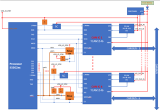
We are using TCAN11446, we want to use RXD pin as wake up source for processor to be woken up.

In sleep mode of TCAN1146 VCC & VIO are not available, we are turning ON VCC & VIO supplies of TACN1146 based on INH pin state.

Please confirm for the above our configuration whether RXD pin ca be used as wake up source for processor to be woken up.


  • Hi Murali,

    When the TCAN1146 is in sleep mode and receives a valid wake condition, the device will automatically move to standby mode and drive the INH signal high. In your system, this will cause Vio and Vcc to become active. Once the Vio rail is available, TCAN1146 will be able to drive the RXD pin low in order to indicate to the MCU that a wake event has occurred.

    Let me know if this sequence will work for yous system or if there is something missing.

    Regards,
    Eric Schott 

  • Hi Eric,

    Thanks for your response. 
    I need more clarity on your response. 
    As I explained in my first post, In sleep mode TCAN1146 --> VCC & VIO are in off state. 
    I understood from the datasheet TCAN1146 RXD pin contains internal pull up connected to VIO. Since VIO in off state during sleep mode.

    Can you confirm following my understanding/queries, so that I will get more clarity on RXD pin usage as sleep to standby mode wake event detection.

    1. I want to know what is the state of RXD pin ( Hi or Low/Floating), during TCAN1146 sleep mode ( VCC & VIO also not available ).

    2. In case  RXD pin is floating in sleep mode( where VCC & VIO not available), do I need a external pull up on RXD pin to detect LOW indication on RXD pin during sleep to standby mode entry?

    3. As per my application (VCC & VIO not available in sleep mode) when TCAN1146 enters to standby mode, the RXD pin first go to high and immediately RXD PIN goes to low LOW, is this correct ?

     Please confirm the above points.

  • Hi Murali,

    I appreciate you working with us to understand this device. 

    1. I want to know what is the state of RXD pin ( Hi or Low/Floating), during TCAN1146 sleep mode ( VCC & VIO also not available ).

    When Vio is not supplied, the RXD pin will remain in a high impedance state. 

    2. In case  RXD pin is floating in sleep mode( where VCC & VIO not available), do I need a external pull up on RXD pin to detect LOW indication on RXD pin during sleep to standby mode entry?

    While the transceiver is in sleep mode, it is assumed that the MCU is off and not capable of monitoring the RXD pin so the pin state is not relevant. Only once the MCU is supplied when Vio returns will the pin state be recognized by the MCU. Because Vio is commonly used by both the transceiver and MCU, this will also mean that Vio is available to the transceiver and the RXD pin is active and can drive low to indicate a wake condition. 

    If the MCU is powered and active while the transceiver is in sleep mode, the RXD pin should include an external pull-up to the supply used by the MCU. 

    3. As per my application (VCC & VIO not available in sleep mode) when TCAN1146 enters to standby mode, the RXD pin first go to high and immediately RXD PIN goes to low LOW, is this correct ?

    The state of the RXD pin will depend on the status of the Vio supply. If Vio is not available in sleep mode, it will also not be active immediately once the transceiver enters standby mode. For the time that the transceiver is in standby with Vio still unavailable, the RXD pin will be high impedance with the internal pull-up to Vio active. During this time if Vio is becoming active, the RXD pin will begin to go high due to this pull-up. Once Vio > UVio, the transceiver will enable the RXD pin and it will be pulled low to indicate the wake event to the MCU.

    Note that the ramp time of the Vio supply is system dependant so the actual voltage that the RXD pin reaches before TCAN1145 can drive the pin state low cannot be specified. If this process is used, the MCU should not be programmed to use a falling edge to wake from its low power state. 

    Overall, if the MCU is active during the sleep mode of the CAN transceiver, then an external pull-up should be used on RXD. If the MCU is powered off during the sleep mode of the transceiver, then a wake event will cause the MCU to be powered on (via INH enabling the MCU power supply) so an edge should not be needed to wake the MCU. 

    Let me know if this is clear and if you have any more questions.

    Regards, 
    Eric Schott 

  • Hi Eric,

    Thanks a lot for your deep explanation. 

    In sleep mode our processor will be in low power mode, in this mode standby supply is available in processor communication ports to detect any interrupt/state change on the communication ports.

    From your message we under stood we need a pull up resistor in RXD Pin because TCAN1146 VCC and VIO are not available in sleep mode.

    Here I have shared our TCAN1146 architecture to your mail ID (e-schott@ti.com) , We are using Qty 6 TCAN1146 IC's in our design.  In architecture diagram only shown 2 TCAN1146.

    We are going to connect QTY 6 TCAN1146 IC's with a single SPI bus to processor with individual chip selects. is this a problem ?

    We need few more details form you regardingTCAN1146 usage, please provide your inputs on following points

    1. We are planning to use following mux SN74LVC1G3157-Q1, for SDO/nINT pin. Can you confirm what is the state of not connected MUX pin whether it is open drain ?

    2. Mux output  of all TCNA1146 nINT pin's, We are plaining to tie all together and connecting to single processor pin with a pull up resistor to detect nINT status change, Please confirm whether we connect like this ?

    3. Please suggest if you have any other mux options which you fell better fit for our application compared to above .

    Thanks & Regards,

    Murali Penta

    mpenta@fiskerinc.com.

  • Hi Murali,

    I agree that the external pull-up to the VCC_IO_STBY on RXD looks good here. This will ensure that the RXD signal is high before the wake up period so a falling edge will be seen by the MCU for the interrupt. 

    For the rest of the questions here, it seems like there's an email thread going on with TI and Manoj that has addressed a lot of the concerns here. Is it possible for you to reference the email thread for there answers? 

    Regards, 
    Eric Schott 

  •  TI Team,

    Since Manoj not available currently, I am writing further queries on TCAN1146 behalf of him.

    As per discussion with Eric Schott in TI forum, we will use TCAN1146 RXD pin as wake events indicator to the MCU.

    We also want to detect other interrupts which are indicated through SDO/nINT pin in normal mode (except sleep to wake indication), because we are using Qty 6 TCAN1146 IC’s, every time polling with SPI bus is difficult in normal mode.

    I have attached our TCAN1146 block diagram FYR. In block diagram we have shown only 2 TCAN1146 IC’s . In actual scenario qty 6 TCAN1146 will be there.

    @e-schott@ti.com the following queries, with respect to nINT pin connection with processor.

     1. We are planning to use following mux SN74LVC1G3157-Q1, control via chip select pin of TCAN1146. Can you confirm what is the state of not selected MUX output ( when chip select is LOW & SDO connected to processor) whether it is open drain ? 

    Also please suggest if you have any other mux options/part numbers which you feel better fit for our application compared to above.

    2. We are connecting nINT signals of all Mux outputs (Qty 6 TCAN1146) together and connecting to a single processor pin with a pull resistor ( Please see in block diagram for clear understanding).

    So that any TCAN1146 IC nINT pin interrupt can detected in normal mode, after that we will start polling through SPI bus to k now the which TCAN1146 generated.

    Do we need pull up resistor at Mux input also ( at TCAN1146 SDO/nINT pin) ?

    Please confirm if you see any issues while tying all TCAN1146 nINT pins together( MUX outputs) and connecting to single processor pin?.

    3. Things mentioned in the datasheet below, will it make any issue for our design , because we are using MUX on SDO/nINT pins of all TCAN1146 IC’s it will isolate the SDO line and nINT line.

  • Hi Murali,

    Sorry for the long delay on this one. In summary of the below responses, I don't see any issue with the proposed solution in the diagram here. 

     1. We are planning to use following mux SN74LVC1G3157-Q1, control via chip select pin of TCAN1146. Can you confirm what is the state of not selected MUX output ( when chip select is LOW & SDO connected to processor) whether it is open drain ? 

    The nINT pin configuration (when nCS is not asserted) is an open drain output with internal pull-up to Vio. This is fine to be muxed with multiple other nINT signals. 

    Do we need pull up resistor at Mux input also ( at TCAN1146 SDO/nINT pin) ?

    Yes, I would recommend including an external pull-up to Vio on the MCU-side of the nINT MUX's.

    Please confirm if you see any issues while tying all TCAN1146 nINT pins together( MUX outputs) and connecting to single processor pin?.

    I see no issue with this solution. 

    3. Things mentioned in the datasheet below, will it make any issue for our design , because we are using MUX on SDO/nINT pins of all TCAN1146 IC’s it will isolate the SDO line and nINT line.

    I'm not sure what is meant by this. The MUX solution for the nINT and SDO signals is included as an example in the datasheet in figure 10-6. I don't see any issue combining the nINT signals on the MCU-side of the MUX's when multiple TCAN1146s are used in the same application. 

    Regards,
    Eric Schott

  • Hi TI Eric Schott,

    Thanks for the response. 

    Can we get load dump and jump start test report for this  CAN IC - TCAN1146-Q1  ?

    Thanks & Regards, 

    Murali Penta

  • Hi Murali,

    These are pretty general descriptions of tests that I'm not sure we have a general report for. Is there a specific test standard that you are referencing for this information? 

    The test reports we make publicly available are for C&S interoperability, J2962 compliance (NA), and Zwickau EMC (EU). If you need any of these or other specific standard test numbers, I can send them to you via email. Please let me know what is of interest for you and confirm that I may send any of this information to the email associated with your E2E account.

    Regards, 
    Eric Schott