Part Number: TSB41BA3A
Need clarification
Datasheet pg 18 states JC of 0.17 C/W with bottom soldered to pad on board
Also state 0.17 C/W if the bottom is not soldered to board
Doesn't seem to make sense that they are the same. Is the JC for both to the metal pad on the base or the leads, and
is the grounding scheme on page 28 required for the TPFPEP version of the device.
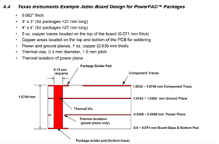
Data also say JC valid on "High conductivity Texas Instruments recommended test board" but doesn't clearly define. I assume
themal pad on board for both the places this is defined, but does it require 2 oz copper in the board? Deissipation Rating Table on
page 15 mentions 2 oz "traces" for these configurations but traces are usually exterior layers of bd