This thread has been locked.

If you have a related question, please click the "Ask a related question" button in the top right corner. The newly created question will be automatically linked to this question.

TCA9509:How to use TCA9509

Part Number: TCA9509
Other Parts Discussed in Thread: LSF0102, TCA9511A, TCA4307, LSF0101, TCA9517A, TCA9545A

Hi There,

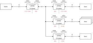
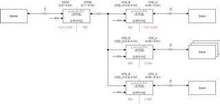
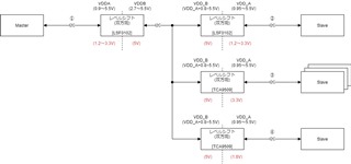
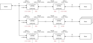
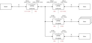
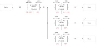
I plan to use the TCA9509.
The TCA9509 is capable of series and star connections on the B-side connection.
I am considering the circuit configuration of the file with I2C.

Are there any problems with the TCA9509?

Best regards
- satoshi

plan (動) 計画する、予定する、考える、画策する、企画する、企む、考案する

plan (名) 予定、計画、プラン、構想

Powered by iKnow!
  • This will work. (The only restrictions are on the A-side I/Os.)

  • Hi Ladisch,


    What is the A-Side I/O restrictions?
    Do you mean the content of the 10.1 Application Information?
    In summary, is it correct to pull the A port VIH sufficiently low?

    Best regards
    - satoshi

  • Yes; you cannot connect A-side I/Os to other special I²C ports (such as the A side of other TCA9509s, or ports with voltage offset of other I²C buffers), and you must not use pull-up resistors. (Also see section 10.2.1.)

  • Hi Ladisch,

    Thank you for your reply.
    This system has pull-up resistors in ① and ② (top route), making it difficult to realization the circuit configuration.
    Is there a good device that doesn't have pull-up restrictions?

    ※I'd like to avoid switches such as the LSF0102 because the load capacity increases with multiple stages.

    The document added numbers to the I2C paths.

    Best regards
    - satoshi

  • All the other I²C buffers that allow translation between 1.2 V and 5 V (TCA9517x, TCA9617x) have the special port on the B side, so they do not work in this star connection.

    The TCA9511A or TCA4307 would work, but only with at least 2.5 V.

  • Hi Satoshi,

    Clemens is correct. The TCA9509 has voltage contention restrictions only present on the A-side which presents other A-side from TCA9509 to be connected together, or any other devices that implements some voltage offset that could interfere with the VILC spec. This also includes pull-up resistors as Clemens mentioned, which means nodes 1/2/3/4 need pull-up resistors removed. 

    If you are looking for an alternative device for this, we recommend the TCA9511A over the TCA4307. Both the 9511A and the 4307 do not implement voltage level translation. 

    May I ask why you are using multiple 9509 buffers in your application? Are you nearing the 400pF bus capacitance limit for I2C standards? How many devices are on the slave side? Would you be able to generate a solution with an I2C controlled switch in place of the 9509 that would allow you to turn on/off specific channels in order to separate the bus capacitance from the master side vs. the slave side? 

    Regards,

    Tyler

  • Hi Clemens and Tyler

    Thanks for all the advice.
    I need to level convert the low voltage and can't use the TCA9511A.

    Slave devices will be 1 slave device for ②, 5 for ③, and 1 for ④.
    Therefore, I2C controlled switches have tight load capacities.
    However, any suggestions to turn each channel on/off would be very helpful.
    I'd like to consider that configuration as well.

    We will continue to consider the following two proposals.


     When using the control switch only for ① and ②


    When using a control switch

    Best regards
    - satoshi

  • Hi Satoshi,

    For the first case, 4 x LSF0102 switches are used, but the EN connection is all one net. Is this a bad representation of the EN pin, or is it true that only one EN input will control all four switches? If this is the case, then all the switches would be connected to the I2C bus, meaning that all 7 slave devices would be loading the I2C bus upon the EN pin being toggled. LSF0102 is a passive device, and is does not have true buffering capability. Parallel parasitic capacitance from each branch (2/3/4) would combine. 

    In scenario 2, implementation of the TCA9509 would work as this would buffer the parasitic capacitance from slave branches 3 and 4 from the main I2C bus connecting to the MCU. This would help with separating the parasitic bus capacitance so that the total bus cap doesn't near the 400pF limit. 

    Regards,

    Tyler

  • Hi Tyler

    For the first case, Wrong enable connection.
    Correctly, we considered controlling only the latter stage level shifter and individual enable control.
    However, I could not control the enable with Pspice.
    Enable control was possible when branching from the level shifter in the previous stage.
    If you know the cause, please let me know.
    ※I replaced it with LSF0101 and simulated

    Scenario 2 is the likely candidate.
    Currently, it is a configuration that can drive while adjusting the pull-up current in the route from ① to ②.
    If the pull-up current is about 1mA, it seems to be able to operate at 400kHz.

    I examined the circuit configuration with the understanding that there are no restrictions on the B port.
    Please let me know if you have any issues.

    Best regards
    - satoshi

  • Hi Satoshi,

    In this new design you provided, you removed the 2 x TCA9509 buffering devices and replaced everything with LSF0102. The LSF0102 is not a true buffer. It will not be able to buffer the I2C lines and separate the bus capacitance from the slave side to the master side. It it redundant to use two of these LSF0102 in series. 

    My suggestion is to use something like the TCA9545A which is a 4 channel I2C controlled switch and buffer combo such as the TCA9517A. 

    Connection will go as follows:

    master -> TCA9545A -> 3 x TCA9517A buffers (1 buffer / slave branch) -> slave devices 

    Regards,

    Tyler

  • Hi Tyler

    Sorry for the confusion.
    This is the result of considering the proposed ON/OFF configuration.
    The method of configuring everything with LSF0102 is not adopted.
    Also, the TCA9545A cannot be used because it must operate at 1.2V.

    Scenario 2 is the likely candidate.
    Let me know if you have any concerns about this configuration.

    ① and ② have pull-ups, and ③ and ④ do not.
    There is also a pull-up between LSF0102-LSF0102.

    Best regards
    - satoshi

  • Hi Satoshi,

    This configuration looks like it will work. TCA9509 will buffer sides 3 and 4 from the main I2C bus. The LSF devices are not true buffers. The only way to separate the bus capacitance with those devices is to disable them when the master does not need to communicate with downstream slave devices on

    It is recommended to have pull-up resistors present on the node that connects the 2 x LSF and 2 x 9509 devices. There is no internal biasing present on that side, and will need external pull-up resistors. 

    Otherwise this configuration looks ok to me.

    Regards,

    Tyler

  • Hi Tyler

    Thanks to Tyler, I was able to determine the circuit configuration.
    Thanks for all the technical advice.

    Best regards
    - satoshi