This thread has been locked.

If you have a related question, please click the "Ask a related question" button in the top right corner. The newly created question will be automatically linked to this question.

SN65HVD72: Short circuit behaviour analysis

Part Number: SN65HVD72

Hi team, 

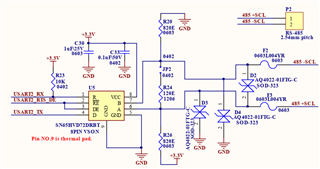
We are using SN65HVD72DRBT in our product with the 40mA PPTC on the Differential line.

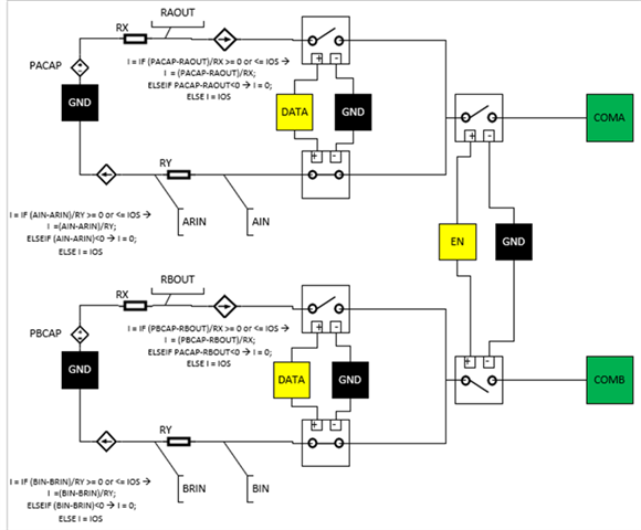
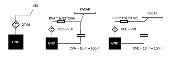
We need to analyze the short circuit behavior of the Differential Bus with and without termination and failsafe resistors.

As, I got to know from support, SPICE model for the IC is not available, and with the IBIS model, I cannot simulate the short circuit behavior with the Altium designer tool.

Please guide through the same, to analyze the short circuit behavior modelling of the same. 

Thanks, 

Rishav

  • Hi Rishav,

    Is it possible to share what the differential bus looks like - as the positioning on the fuse will impact analysis and I don't want to assume incorrectly where it is placed.

    That being said - essentially the current limit is just that - it limits the current to sink/source no more than 160mA for this device.  If we neglect the cabling for the bus and just focus on the transceiver + terminations + failsafe resistors - the bus becomes a simple resistor network. Largely this is how our newer spice models are built - and we put a current limiter on the outputs/inputs of the transceiver pins that when they hit the datasheet values they limit current at that value - and its a hard stop with the models. Up until they hit that point though it is a simple linear resistance network and the current drawn from the driver is proportional to the load.

    Are you trying to adequately size the fuse for the application? If so - could you also answer the following questions:

    1. How long is the maximum  bus length.

    2. How many communication nodes are going to be present on the bus (maximum)

    3. What data-rate are you running the system at? (increases in data-rate increase current output) 

    Please let me know !

    Best,

    Parker Dodson

  • Hi Parker, 

    Please, find the schematic for fuse position 

    Further, 

    1. How long is the maximum bus length.

    Standard rs485 length ~1000m

    2. How many communication nodes are going to be present on the bus (maximum)

    32

    3. What data-rate are you running the system at? (increases in data-rate increase current output)

    115200

    The agenda for the analysis is two fold, first to rationalize the fuse rating and second to calculate the total energy at the bus in case of short circuit, for certification purpose.

    I was considering modelling the circuit in terms of voltage source and resistor, Please suggest the way forward.

    Thanks, 

    Rishav 

  • Hi Rishav,

    Alright - that makes sense.

    So I will just share how to model the output driver in a pretty simple way - I will say due to the nature of the driver a strict Voltage source and Resistor will not work - as it doesn't model the non-linear current limiter - so generally you have to have spice file - but the driver itself isn't that complicated and I can show you what the spice file would look like

    This shows the driver with a current limit modeled in a simple fashion using dependent sources, resistors, and switches. 

    Essentially the RX and RY values are used to set VOD and VOC specs (output differential and output common voltages).

    PACAP and PBCAP act as our source - their max value is the approximated open circuit voltage of the driver (as a RS-485 driver at no load will output ~VCC - 2 diode voltage drops) - but they have a built in RC rise/fall delay to mimic the transition time of the driver - that is explained in the model image - but if you aren't as concerned with timing you can just replace PBCAP and PACAP with voltage sources equal to VCC - 2 diode drops - since this device doesn't have an open circuit VOD specification I would use 0.3V as the diode drop value and the voltage sources can be set to VCC - 0.6V.

    The dependent current sources essentially do nothing but limit current when you hit the IOS value in datasheet (which occurs at shorts - or very low impedances). There is a lot of text around them but essentially - they measure the voltage across RX or RY and convert that to a current - if the current is between 0A and IOS limit then the current is exactly as expected of a linear system - it adds some diode functionality by not allowing current backflow - i.e. if a current would be under 0A it will not conduct current and if the current draw is greater than IOS it will not output more than IOS. 

    The equations of RX and RY are shown below  with the following constants: vs = VCC - 2*vd ; rt(spec) = 54 ; rcm(spec) = 375

    This process will size RX and RY - one thing to note is that there will be error with respect to datasheet on both VOD and VOC since this model doesn't typically line up perfectly with the actual device. Usually the error is small (<5%) but at higher loading and common mode inputs you could see up to ~ +/-7% error - for short circuit testing however this really shouldn't be much of a problem. 

    For this device typically you would expect VOD to be 2V and VOC(ss) to be 1.65V (assuming 3.3V supply) - so that would yield resistor sizing's of:

    RX = 0.856 Ohms

    RY = 16.774 Ohms

    To ensure that the proper IOS limit is set we should also calculate the voltage across RX and RY when IOS is ran through them (160mA for this device) 

    So V_RX_IOS = 136.96mV

    and V_RY_IOS = 2.68384V

    If you want to include transition time in the simulation you  will need to add the following other circuits:

    RVB and RVA are an approximate value - if you are just looking for a simple model I'd forgo this portion as its finicky and usually requires multiple iterations before the timing works well - but this is how the transition time could be modeled. If we were to model it for this device the first past would use CVA and CVB = 10nF and RVB = RVA = 35 Ohms - however this may need to be varied to hit correct results - so if you can not use this in the model it would most likely be beneficial.

    The spice model for this will take the general form as shown below (I have used the numbers we calculated in the example above)

    """

    *Driver Output with current limit - includes transition time

    .subckt DiffDriverWIlim VCC EN DATA A B GND
    XDRIVE VCC GND AOUT BIN BOUT AIN DATA diffDriver
    XDECIDE EN DATA AOUT BOUT AIN BIN A B GND DRIVEMATRIX
    .ENDS


    .subckt diffDriver VCC GND AOUT BIN BOUT AIN DATA
    VDUBDIODE VDI GND 0.6
    EVABASE PABASE GND VALUE = {IF( V(DATA,GND) > 0.37, V(VCC,VDI), 0)}
    EVBBASE PBBASE GND VALUE = {IF( V(DATA,GND) < 0.63, V(VCC,VDI), 0)}
    RVA PABASE PACAP 35
    RVB PBBASE PBCAP 35
    CVA PACAP GND 10E-9
    CVB PBCAP GND 10E-9
    EVAOUT PAOUT GND VALUE = {V(PACAP,GND)}
    EVBOUT PBOUT GND VALUE = {V(PBCAP,GND)}
    GAOUT RAOUT AOUT VALUE = { IF( (V(PAOUT,RAOUT)) > 0.13696, 0.16, IF( V(PAOUT,RAOUT) < 0, 0, V(PAOUT,RAOUT) / 0.856)) }
    GBOUT RBOUT BOUT VALUE = { IF( (V(PBOUT,RBOUT)) > 0.13696, 0.16, IF( V(PBOUT,RBOUT) < 0, 0, V(PBOUT,RBOUT) / 0.856)) }
    GAI ARIN GND VALUE = { IF( (V(AIN,ARIN)) > 2.68384, 0.16, IF( V(AIN,ARIN) < 0, 0, V(AIN,ARIN) / 16.774)) }
    GBI BRIN GND VALUE = { IF( (V(BIN,BRIN)) > 2.68384, 0.16, IF( V(BIN,BRIN) < 0, 0, V(BIN,BRIN) / 16.774)) }
    RXA PAOUT RAOUT 0.856
    RYA AIN ARIN 16.774
    RXB PBOUT RBOUT 0.856
    RYB BIN BRIN 16.774
    .ENDS


    .subckt DRIVEMATRIX EN DATA INA INB OUTA OUTB COMA COMB GND
    EVNDATA NDATA GND VALUE = { IF (V(DATA,GND) > 0.63, 0, 1) }

    S1 INA COMAA DATA GND SWON
    S2 OUTA COMAA DATA GND SWOFF
    S3 INB COMBB DATA GND SWOFF
    S4 OUTB COMBB DATA GND SWON
    S5 COMBB COMB EN GND SWON
    S6 COMAA COMA EN GND SWON

    .MODEL SWON VSWITCH Roff=1e9 Ron=0.001 Voff=0.37V Von=0.63V
    .MODEL SWOFF VSWITCH Roff=1e9 Ron=0.001 Voff=0.63V Von=0.37V
    .ENDS

    """

    And if you want to remove the transition time aspect so to prevent iterative design on the model it would just be:

    """

    *Driver with current limit without transition time 

    .subckt DiffDriverWIlim VCC EN DATA A B GND
    XDRIVE VCC GND AOUT BIN BOUT AIN DATA diffDriver
    XDECIDE EN DATA AOUT BOUT AIN BIN A B GND DRIVEMATRIX
    .ENDS


    .subckt diffDriver VCC GND AOUT BIN BOUT AIN DATA
    VDUBDIODE VDI GND 0.6
    EVABASE PABASE GND VALUE = {IF( V(DATA,GND) > 0.37, V(VCC,VDI), 0)}
    EVBBASE PBBASE GND VALUE = {IF( V(DATA,GND) < 0.63, V(VCC,VDI), 0)}
    EVAOUT PAOUT GND VALUE = {V(PABASE,GND)}
    EVBOUT PBOUT GND VALUE = {V(PBBASE,GND)}
    GAOUT RAOUT AOUT VALUE = { IF( (V(PAOUT,RAOUT)) > 0.13696, 0.16, IF( V(PAOUT,RAOUT) < 0, 0, V(PAOUT,RAOUT) / 0.856)) }
    GBOUT RBOUT BOUT VALUE = { IF( (V(PBOUT,RBOUT)) > 0.13696, 0.16, IF( V(PBOUT,RBOUT) < 0, 0, V(PBOUT,RBOUT) / 0.856)) }
    GAI ARIN GND VALUE = { IF( (V(AIN,ARIN)) > 2.68384, 0.16, IF( V(AIN,ARIN) < 0, 0, V(AIN,ARIN) / 16.774)) }
    GBI BRIN GND VALUE = { IF( (V(BIN,BRIN)) > 2.68384, 0.16, IF( V(BIN,BRIN) < 0, 0, V(BIN,BRIN) / 16.774)) }
    RXA PAOUT RAOUT 0.856
    RYA AIN ARIN 16.774
    RXB PBOUT RBOUT 0.856
    RYB BIN BRIN 16.774
    .ENDS


    .subckt DRIVEMATRIX EN DATA INA INB OUTA OUTB COMA COMB GND
    EVNDATA NDATA GND VALUE = { IF (V(DATA,GND) > 0.63, 0, 1) }

    S1 INA COMAA DATA GND SWON
    S2 OUTA COMAA DATA GND SWOFF
    S3 INB COMBB DATA GND SWOFF
    S4 OUTB COMBB DATA GND SWON
    S5 COMBB COMB EN GND SWON
    S6 COMAA COMA EN GND SWON

    .MODEL SWON VSWITCH Roff=1e9 Ron=0.001 Voff=0.37V Von=0.63V
    .MODEL SWOFF VSWITCH Roff=1e9 Ron=0.001 Voff=0.63V Von=0.37V
    .END

    """

    You should just be able to copy this text and save it as a .lib file and import into your preferred spice simulator (except HSpice - it won't probably work on that one) 

    A few notes - this model doesn't capture propagation delays, nor receiver loading - so its far from a complete model, but it does model the current limit and output voltages (and transition time of the differential signal) and should be beneficial in your simulation needs.

    A major use note is that the DATA (also known as D pins on most RS-485) and the EN (a stand-in for DE pins on most RS-485) are expecting values between 0V and 1V and if you use higher voltages you will get weird results (this is because as a partial model we are missing the logic to bus interface circuits which convert logic signals to high or low values with low voltages for simplicity - so the model is assuming inputs of 0v to 1V on the DATA and EN inputs. 

    Please let me know if you have any other questions and I will see what I can do - this model hasn't been vetted obviously since its a very simplified version - but based on test setups - this model will be decently accurate for the actual voltages and should help you understand energy use in the circuit a bit better than without any model.

    Best,

    Parker Dodson