This thread has been locked.

If you have a related question, please click the "Ask a related question" button in the top right corner. The newly created question will be automatically linked to this question.

MAX3221: Noise problems with new date code

Part Number: MAX3221

Hi,

I have a design that uses the MAX3221 interface chip. The design has been stable for a number of years, but has recently started to present problems, which was traced to an increase in noise on our 5V rail when a new batch of MAX3221 chips was used. Swapping the chip back to one with an older date code appeared to reduce the noise and fix the problem.

On a related thread it was mentioned that a die change had happened about a year or so ago MAX3221: MFR differences - Interface forum - Interface - TI E2E support forums. I have a couple of questions:

What did this change do to the switching performance of the switches in the charge pump?

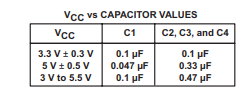
Has TI changed its recommended filtering for the chip? (Note, using the datasheet recommended 100nF cap on Vcc we get more than 700mV pp noise)

Was a PCN issued for this change?

Q.K.

  • That was PCN# 20210720000.1.

    I don't know anything, but it's possible that the new die uses switches with lower on-resistance, resulting in larger current spikes.

    In theory, designed the circuit according to the datasheet recommendations should work. Please show the board layout, especially the five capacitors.

  • Hi Quinn,

    As Clemens mentioned there was a PCN for this device (it is related to the fabrication site change - as mentioned in linked post).

    So the answer to your question - is there could be differences in performance, but if we don't have a characterized specification for that in the datasheet for this device it may not be captured as a change. We don't have a noise spec - and really don't spec much about the charge pump at all in our RS-232 devices - so there could be some change.

    That being said I do have a few questions:

    1. Have you measured the frequency of the noise? 

    2. What sizing of caps did you use for C1,C2, C3, and C4? 

    3. Is it possible to show the layout of the IC - mainly just the VCC line and around the Capacitors for the charge pump? I understand if you can't on the forum - but it would be very helpful to see if there is a potential layout issue.

    4. Have you tried a slightly larger supply decoupling capacitor - like 270nF or 330nF? There generally isn't a lot of risk for a slight increase - and you may just need to increase the capacity of the decoupling capacitor a bit to help reduce the noise on the line. As there could be a difference in actual specifications of the device that don't mesh with the specific specific system is used in.

    Just as a note -we haven't changed our recommendations - but that doesn't necessarily mean that 100% absolute certainty there could be exceptions raised due to uncharacterized part changes in specific systems. All of our tests are simplified approximate models of real systems - but we use RC loading - no silicon and no cabling is included generally - so there always is a potential for an edge case. 

    Please let me know on the few questions and I will see if we can help diagnose the issue.

    Best,

    Parker Dodson 

  • Hi Parker,

    Thank you for your reply, I think you have confirmed I am on the right track. It took a while to track down but I found the PCN via Mouser's website.

    In answer to your questions, the noise spikes appear to occur at a rate of around 18kHz, when the RS232 is communicating.

    C1 is 100nF and C2-C4 are all 330nF. It is a legacy design so I'm not sure why these values were chosen, but in case you were wondering reducing C1 to 47nF does help a bit.

    The layout is not ideal, but as it is a legacy product I am inclined to leave it well alone. The MAX3221 is mounted top-side with C1-C4 all placed and wired tight to the chip, but C_bypass is mounted bottom-side 5mm from the MAX3221 supply pins.  Vcc is run direct. The GND path from C_bypass is via a plane layer but is shared with the GND return from our microcontroller. Occasionally this micro detects a spurious fault condition (probably via one of two analogue inputs). Soldering 100nF directly across pins 14 & 15 of the MAX3221 greatly improves the problem but doesn't eliminate it.

    Increasing the decoupling helps. 220nF was not quite enough in our application. With 470nF fitted it ran for more than 7 hours with no faults. As 1uF and 2u2 gave similar fault free operation I have changed the decoupling to 1uF to give myself some margin.

    Quinn

  • C1 and C2 are the switching capacitors; increasing or decreasing them will increase/decrease the ripple on VCC and the output voltages. (If they are too small, the output voltages will sag under load. You could try to find out how low you can go, but you need a safety factor for temperature and manufacturing variations.)

    C3 and C4 are decoupling capacitors for the output voltages; if you make them larger, the output will have smaller ripple, but startup will be slower.

    CBYPASS is the decoupling capacitor for the input. A larger value will decrease the ripple on VCC; you can make it as large as you want, as long as your power supply can handle it.

  • HI Quinn,

    So based on your response - I think a decoupling cap of 1uF should be fine as Clemens mentioned as long as your power supply can handle it the part really won't mind and based on the soak test I think that more or less confirms that.

    As you mentioned reducing C1 to 47nF helps a bit - as that does better match our recommendations  so that makes sense. 

    So I think your solution makes sense and I do think this is the best solution moving forward.

    Please let me know if you have any other questions!

    Best,

    Parker Dodson