Dear Team,
We are considering to use DP83TC812R chip for 100-base T1 functionality. Our architecture involves converting PCIe to MII with LAN7431 IC from microchip and the DP83TC812R is interfaced with LAN7431 through MII interface.
Could you please clarify the following questions to procced with our design?
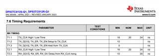
Q1. The high / low times for the TX clock (output clock) as per the datasheet appears to be ranging from 16ns to 24ns. MII interfaces works at constant 25MHz and ton + toff would need to 40ns(time period for 25MHz). So when ton is 16ns , then toff must be 24ns and vice versa. Could you please confirm our understanding on this?

Q2. Upon checking the pin to pin connection for MII interface, in DP83TC812R chip, there is no availability of these pins (CRS, COL, TX_ER). Due to lack of these pins could you please us how these pins must be handled from the MAC (LAN7431)? Also could you please confirm whether DP83TC812R is compatible MII mode without these pins?
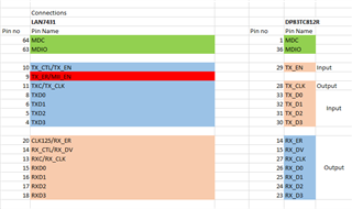
Q3. With the available pins for MII we have planned to map the pins of DP83TC812R & LAN7431 as shown in the following image. Please check and let us know whether it is fine?

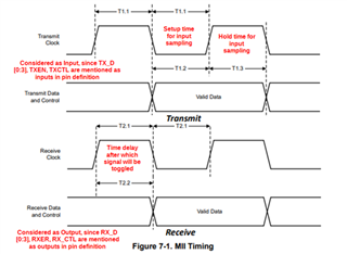
Q4. In timing diagram, the Transmit section as mentioned as input to DP83TC812R and the receive section is the output from DP83TC812R. Please check our understanding in the following image and confirm whether our understanding is correct?

Q5. Since we are planning to interface DP83TC812R which is an 100base-T1 to LAN7431 (PCIe to MII) do we need to take care anything in particular with respect to software and hardware other than the above mentioned queries?
Thanks,
Dharaneshwar S

