This thread has been locked.

If you have a related question, please click the "Ask a related question" button in the top right corner. The newly created question will be automatically linked to this question.

TIOL1123: Compatibility with microcontrollers and IO-Link Devices

Part Number: TIOL1123
Other Parts Discussed in Thread: TIOL112, BOOSTXL-IOLINKM-8

Hi,

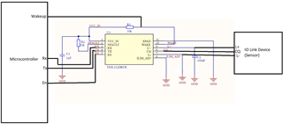
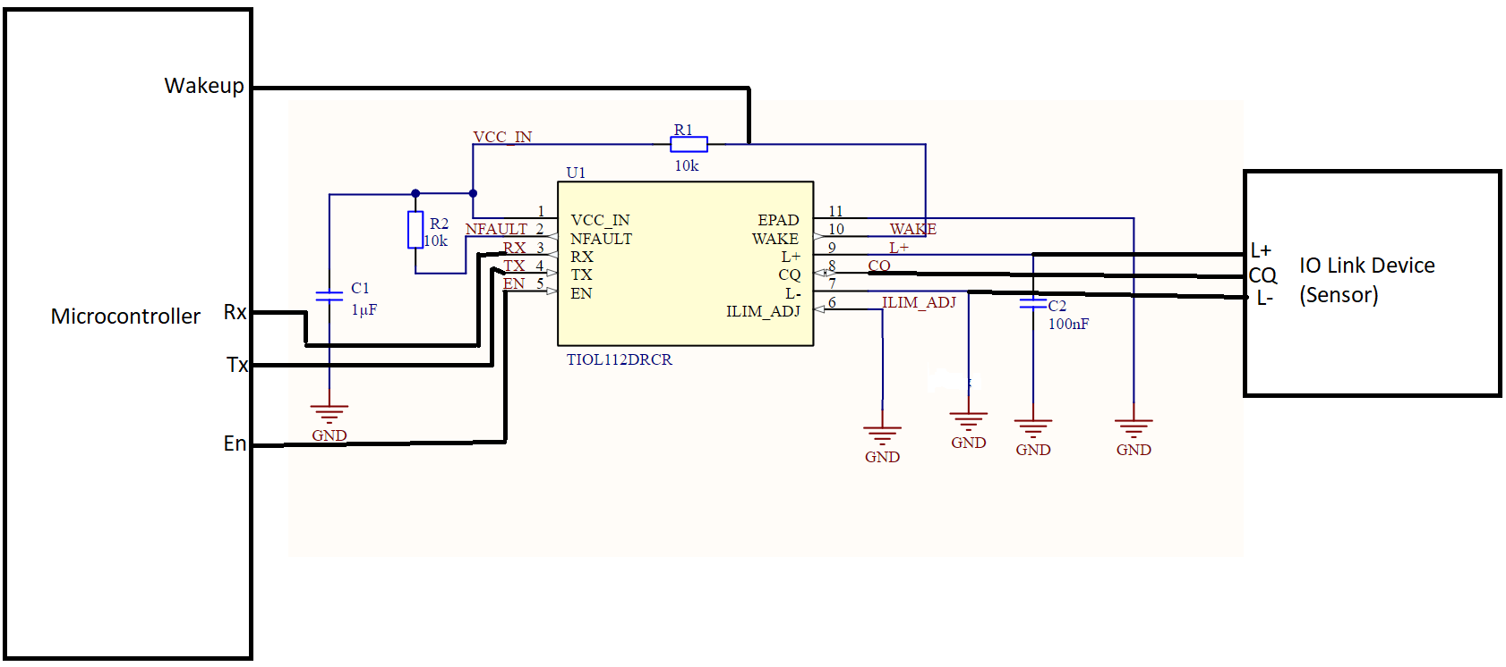
I want to read and write data from IO-Link device that is a sensor to measure Temperature and Flow rate. The Microcontroller can not directly connect to IO-Link device so found this TIOL1123 Transceiver. But the datasheet is not clear about its typical applications. Like can it be used in a way that I can read or write data like configuration and measurements from IO-Link device if the IO-Link device is connected to this TIOL1123 Transceiver and EN, TX, RX, NFAULT and WAKE pins are connected to the microcontroller. Is this what the typical application of this Transceiver??

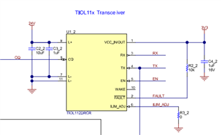
I am not clear about role of this Transceiver is it a Master or not? As per datasheet it can be used in Master Mode if ILIM_ADJ pin is shorted to ground. 

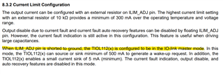
But what mode will it be operating if this pin is not connected to ground?


Thank you

  • Hello,

    IO-Link is an Open Standard protocol designed to standardize communication with sensors and actuators.  You can find all of the information you need on the IO-Link website including overview information and download the standard documents themselves.

    With IO-Link there is a Controller side called a "Master" and a "Device" side of the cable that is the sensor or actuator device you are working with.  The TIOL1123 transceiver is designed to be used in either the Master or Device side applications and it will translate the Digital voltage levels from the microcontrollers (3.3V or 5V) to the 24V industrial signal levels required on the IO-Link cable.  On a simplest level, these transceivers can be though of like special level translators with a few additional features needed to support the IO-Link standard.

    The communication protocol is based on a UART style framework, but the data packets are all defined in the standard itself.  Typically would need to develop or purchase an IO-Link driver firmware stack for your particular microcontroller to handle the IO-Link data protocol for your application.  There are several companies (such as TE Concept as an example) that can provide this firmware stack to speed up your development time.

    IO-Link has a single data wire for communication, but the data is bi-directional so only one side may be controlling or sending data at a time.  If the Device's driver is enabled, but the Master needs to send data to the Device, the Master can drive a current pulse called a Wakeup Pulse on the bus which will be detected by the Device transceiver which will cause the Device to disable the driver and enter a Receive mode so that the Master can transmit the data.  Therefore, there are slightly different requirements for the Master and the Device transceivers with regards to generating this wakeup current pulse.  There is also an integrated 10mA current sink on the Master side to keep a small current flow like a pulldown resistor.

    The TIOL1123 can be placed in to this Master Mode by grounding the ILIM_ADJ pin.  This will enable the 10mA current sink and allow the transceiver to drive higher current levels (>500mA) for the wakeup pulse.  For Device applications, the ILIM_ADJ pin should not be grounded and the resistor value sets the current limit (50mA to 350mA) for how much current can be consumed on the CQ pin.

    Regards,

    Jonathan

  • Thank you for the explanation but the application is still unclear. As per my understating WAKEUP pin on TIOL1123 is an Output pin that is what mentioned in datasheet. 

    So if I am using TIOL1123 as a Master then I need to provide the wakeup pulse from my microcontroller to the wakeup pin on TIOL1123. If I ground ILIM_ADJ is grounded then Wakeup pin will act as Input that means I can WAKEUP my IO LINK device from my microcontroller because then TIOL1123 is in master mode? 
    So as per IO LINK specification I will provide the wakeup current pulse to this wakeup pin on TIOL1123 and then wait for some time as per IO LINK specification and then send some msg to IO Link device and read the response back. 

    The typical application diagram provided in the datasheet is indicating device implementation of TIOL1123. 

    I want to use it as Master so as per my understanding the typical application diagram will look something like this.


    If I am wrong then can you please provide a typical application diagram to use TIOL1123 as MASTER?

    Thank you

  • Hello Tech 00,

    The WAKE pin is an output pin and is only used on the Device side of the IO-Link cable.  It can be left disconnected when used in a Master application. 

    If the Device's CQ driver is enabled and the Master needs to take control of the line, the Master will drive a current pulse in the opposite configuration as the current state of the bus.  This means that the Master could either source or sink a pulse of current that is >500mA for approximately 100us.  The TIOL112's Wake Pulse detection window is between 45us and 145us.  If the TIOL1123 detects such a current pulse while that is within this detection window, it will pull the WAKE pin low.  However, if the current pulse is too short or too long the WAKE pin will remain high. 

    Grounding the ILIM_ADJ pin on the TIOL1123 allows it to produce this larger current for the wake up pulse which needs to be >500mA.  When the ILIM_ADJ pin has a resistor that is >5k to GND, the current will be limited to 350mA or less as required for a Device application.

    For a reference application I would suggest you review the Eight port IO-Link master BoosterPack (BOOSTXL-IOLINKM-8) which is an 8-port Master design implemented for the Sitara AM243 processor and mates with the LP-AM243 LaunchPad

    Full schematic, layout, and BOM information for the BOOSTXL-IOLINKM-8 can be found in the BOOSTXL-IOLINKM-8 EVM User's Guide.

    Additional information about the design as a whole can be found in the Eight Port IO-Link Master Reference Design Guide.

    Regards,

    Jonathan

  • I can explain my question again.

    I have an IO-Link sensor and I want to read measurement data from this IO-Link sensor. So I found this TIOL1123 Transceiver which can be used in Master Mode as per the sheet. So if I implement some very basic IO-Link communication protocol like sending a Wakeup pulse followed by start msgs then my Io Link sensor should wakeup and send me response. 
    So my implementation is like this

    Where microcontroller along with TIOL is acting as Master, as TIOL will not do anything by itself so I have to provide a wakeup signal from microcontroller to TIOL1123 which will the give this Wakeup signal to my IO Link sensor and it will start and respond. But the problem is that the Wakeup can only be used as Output. 
    So now how can I send wakeup request to my IO Link sensor in this configuration? 

    If this is wrong configuration then what is correct?

    Thank you

  • Because you are not working with a full IO-Link firmware stack, you will need to implement the minimum required communication protocol functions yourself, which does include the ability to generate a wake up pulse.  

    The WAKE pin is not used in a Master application, so it can be left unconnected in your schematic.  Here is the TIOL112 implementation in the BOOSTXL-IOLINKM-8 Master BoosterPack.  The CQ net is connected to the IO-Link M12 connector, and the other digital signals (RX, TX, EN, and FAULT) are connected to the MCU.  You will notice the WAKE pin is not used.

    To generate a wake up pulse, the processor should first check the RX pin to determine the state of the CQ line, and then drive the TX pin such that it pulls the CQ line in the opposite polarity of it's current state for a short pulse that is approximately 80uS in length.  You can find the logic tables in the datasheet that will show the relationship between the RX, TX, and CQ voltage levels.  Note that there is an inversion between the RX/TX logic value and the CQ voltage.  In example, when RX/TX=Low, CQ=High, and when RX/TX = High, CQ=Low.

    Figure 7.6 illustrates the CQ, RX and WAKE signal relationship.  This is what the Device is expecting, so your Master application will have to drive the CQ signal to such that the Device will recognize the wake up pulse and causes the Device's WAKE pin to toggle Low as an interrupt for the Device MCU to disable the CQ driver and wait to receive data from the Master.

    Regards,

    Jonathan

  • Thanks a lot for detailed explanation. 

  • You're welcome.  Let us know if you have any other questions about the TIOL1123.

    Regards,

    Jonathan

  • Jonathan will be out of office on vacation until Wednesday next week, thank you for your patience.

    Regards,

    Eric Hackett